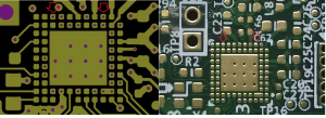
PCB Via in Pad technology, In high-density PCB (Printed Circuit Board) design, Via in Pad (VIP) , some also call it via on pad or VIPPO, technology is a crucial technique used to improve electrical performance, save space, and enhance thermal management. This method involves placing vias directly under component pads, unlike traditional vias that are routed outside pad areas. VIP technology is widely used in applications that require high-speed signals, miniaturization, and improved heat dissipation, such as smartphones, laptops, and aerospace electronics.
Via in Pad
Understanding Via in Pad Technology
1. Definition of Via in Pad
A via is a hole drilled through the PCB layers to establish electrical connections between different layers. Traditionally, vias are placed outside component pads to prevent solder wicking, which can cause reliability issues. However, Via in Pad (VIP) technology involves placing vias directly within the pad areas where components will be soldered.
2. Types of Vias Used in VIP Technology
- Through-Hole Vias: Extend from the top layer to the bottom layer of the PCB.
- Blind Vias: Connect an outer layer to one or more inner layers but do not go through the entire board.
- Buried Vias: Connect inner layers without reaching the surface layers.
- Micro Vias: Small vias typically used in HDI (High-Density Interconnect) designs to improve routing density.
Advantages of Via in Pad Technology
1. Space Optimization
Modern electronic devices demand smaller and more compact PCB layouts. VIP technology eliminates the need for additional routing space, making it possible to fit more components into a smaller area.
2. Improved Electrical Performance
VIP technology helps reduce signal path lengths, minimizing inductance and resistance. This results in better signal integrity, especially in high-speed and high-frequency applications.
3. Better Thermal Dissipation
For power components such as processors and RF modules, effective heat dissipation is essential. Vias in pads help transfer heat efficiently to internal or bottom layers, preventing overheating and improving performance.
4. Enhanced Reliability
Compared to conventional vias, VIP technology offers superior mechanical stability and reduces electromagnetic interference (EMI), improving the durability and reliability of the PCB.
Challenges and Considerations
Despite its advantages, Via in Pad technology also presents challenges that designers and manufacturers must address.
1. Solder Wicking Issues
One major concern is solder wicking, where solder flows into the via hole, leading to weak joints or insufficient solder on the pad. To prevent this, via filling techniques such as non-conductive epoxy filling or copper plugging are used.
2. Manufacturing Complexity and Cost
VIP technology requires precise fabrication techniques, making the manufacturing process more complex and expensive. Additional processes like via filling, planarization, and extra plating increase production time and cost.
3. Design Constraints
Placing vias within pads requires careful planning to avoid potential thermal stress, current leakage, or mechanical weaknesses. Designers must consider via size, placement, and plating techniques to ensure PCB integrity.
Via Filling and Plating Methods
To prevent solder wicking and ensure proper component soldering, different via filling techniques are employed:
1. Conductive Via Fill
- Filled with copper or silver-based epoxy.
- Provides high electrical conductivity and improved thermal performance.
- Used in power applications and RF circuits.
2. Non-Conductive Via Fill
- Uses resin-based materials to prevent solder wicking.
- Ensures a flat, solderable surface.
- Commonly used in HDI boards.
3. Copper-Plugged Vias
- Vias are filled with copper before being plated over.
- Reduces thermal expansion issues.
- Used in high-power applications.
Applications of Via in Pad Technology
VIP technology is essential for modern electronic devices that require high performance, compact size, and better heat dissipation. Some key applications include:
1. Smartphones and Wearable Devices
With increasing miniaturization, mobile devices benefit significantly from VIP technology by reducing PCB size while maintaining performance.
2. High-Speed Computing and Networking Equipment
Servers, routers, and high-performance computing boards utilize VIP for improved signal integrity and thermal management.
3. Medical and Aerospace Electronics
Reliability is critical in medical devices and aerospace applications, where VIP technology ensures robust electrical connections and durability.
4. Automotive Electronics
Modern vehicles require compact and high-performance electronic control units (ECUs), making VIP an ideal choice.
Best Practices for Implementing Via in Pad Technology
To achieve the best results when designing and manufacturing PCBs with Via in Pad technology, consider the following best practices:
1. Proper Via Filling Selection
Choose the appropriate via filling method based on the PCB’s electrical and thermal requirements.
2. Planarization for Solderability
Ensure that via-filled pads are properly planarized to provide a smooth surface for component placement and soldering.
3. Thermal Management Strategies
Use VIP technology in conjunction with thermal vias and heat sinks to maximize heat dissipation.
4. DFM (Design for Manufacturability) Considerations
Work closely with PCB manufacturers to ensure that design specifications align with fabrication capabilities to avoid production delays and defects.
Conclusion
Via in Pad technology is a revolutionary advancement in PCB design, offering significant benefits such as space-saving, improved electrical performance, better heat dissipation, and enhanced reliability. However, it also presents challenges that require careful design considerations and advanced manufacturing techniques. With continued advancements in electronics, VIP technology will play an even more critical role in high-density, high-speed, and high-performance PCBs, making it a standard feature in next-generation circuit boards.

- long board pcb
- Flexible PCBs
- Special PCB
- Express Printed Circuit Board
- Pcb Prototype
- LED PCB
- PCB
- Printed Circuit Board
- Pcb meaning
- Pcb manufacturer
- Rigid pcb board
- Rigid Flex PCB
 Quote
Quote
 E-mail