Introduction
Printed Circuit Boards (PCBs) are the foundation of modern electronic devices, serving as the backbone for component placement and electrical signal transmission. The PCB-manufacturing process is highly intricate, involving multiple critical stages from design to production and final testing. This article provides a detailed overview of the PCB-manufacturing process, highlighting key steps and advanced technologies that enhance production efficiency and product quality.
As the demand for smaller, faster, and more reliable electronic devices grows, the role of PCB-manufacturing becomes increasingly crucial. The evolution of technology, driven by innovations in telecommunications, computing, automotive, and healthcare industries, requires PCBs that can support complex and high-performance applications. In this landscape, PCB manufacturers must continuously innovate to meet the challenges of tighter design requirements, higher data transmission speeds, and stricter environmental regulations.
At the same time, the push for energy-efficient and sustainable PCB-manufacturing processes is reshaping the industry. With more emphasis on reducing waste, lowering carbon footprints, and utilizing eco-friendly materials, manufacturers are exploring green alternatives in every stage of PCB production. This shift is not only essential for compliance with global regulations but also helps companies gain a competitive advantage in an increasingly environmentally-conscious market.
Furthermore, the increasing complexity of electronic devices, including wearables, automotive systems, and IoT devices, demands advanced PCB technologies. Innovations such as High-Density Interconnect (HDI) boards, flexible PCBs, and advanced surface finishes are enabling these devices to achieve higher performance in smaller form factors. As the market continues to evolve, PCB-manufacturing is expected to play an even more critical role in shaping the future of electronics.
In this article, we will explore the current trends, innovations, and challenges in PCB-manufacturing and how the industry is adapting to the rapidly changing technological landscape.
1. Overview of the PCB Manufacturing Process
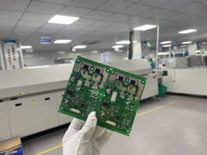
The PCB-manufacturing process typically includes design, material preparation, inner layer processing, lamination, drilling, circuit formation, surface finishing, and final testing. Each stage must be precisely controlled to ensure the reliability and stability of the finished PCB.
PCB-Manufacturing
2. Detailed Breakdown of the PCB-Manufacturing Process
2.1 PCB Design and Material Selection
PCB Design is the starting point of the manufacturing process, and its quality directly impacts the final product’s performance. Key design steps include:
- Schematic Design: Engineers use EDA tools (e.g., Altium Designer, Cadence Allegro) to create circuit diagrams.
- PCB Layout: Components are arranged, and traces are optimized to ensure signal integrity.
- Gerber File Generation: The standard manufacturing format containing information on traces, pads, drill holes, and more.
Material Selection plays a crucial role in PCB performance. Common PCB substrates include:
- FR-4 (Epoxy Glass Fiber): The most widely used PCB material, offering good mechanical and electrical properties.
- High-Frequency Materials (e.g., Rogers PTFE): Suitable for 5G communication and high-speed data transmission.
- Metal Core PCBs (e.g., Aluminum PCB): Used in high-power LED and power amplifier applications for better heat dissipation.
2.2 Inner Layer Processing and Image Transfer
For multilayer PCBs, inner layer circuits are fabricated first. The main steps include:
- Copper Clad Preparation: Cleaning the copper surface to improve adhesion.
- Dry Film Application: A photosensitive dry film is applied to the PCB surface to prepare for imaging.
- Exposure & Development: Using a photomask, the circuit pattern is transferred onto the copper layer, and unwanted areas are removed.
- Etching: Chemical etching removes excess copper, leaving behind the desired circuit pattern.
2.3 Lamination (Layer Stacking)
Multilayer PCBs require a lamination process to bond multiple layers together. Key steps include:
- Layer Alignment: Ensuring precise registration of all layers to prevent misalignment.
- Pressing Process: Under high temperature (180-200°C) and pressure (200-300 PSI), prepreg (semi-cured resin) melts and bonds the layers.
- Cooling & Curing: The PCB structure stabilizes, preventing warping or deformation.
2.4 Drilling and Plating
Drilling is a crucial step that creates vias (interconnections) between layers. Common drilling methods include:
- Mechanical Drilling: Suitable for standard PCBs, with a minimum hole size of 0.15mm.
- Laser Drilling: Used in HDI (High-Density Interconnect) PCBs for microvias as small as 0.05mm.
Plating is necessary to make the vias conductive. Key processes include:
- Electroless Copper Deposition: A thin copper layer is chemically deposited inside the drilled holes.
- Electroplating Copper: Electrolytic copper plating thickens the deposited copper, ensuring strong electrical conductivity.
2.5 Outer Layer Circuit Formation
The process for outer layers is similar to inner layers but requires additional precision. Steps include:
- Photoresist Coating: A light-sensitive film is applied to prepare for pattern transfer.
- Exposure & Development: UV light transfers the circuit pattern onto the outer copper layer.
- Pattern Plating: Copper is electroplated onto the exposed areas to enhance trace thickness.
- Etching: Unwanted copper is chemically removed, leaving behind the final circuit pattern.
2.6 Solder Mask Application and Silkscreen Printing
Solder Mask is an insulating layer that protects copper traces from oxidation and prevents solder bridging during assembly. Common solder mask colors include green, blue, and black. The application methods include:
- Silkscreen Printing: Applying solder mask ink through a stencil.
- Spray Coating: Used for high-precision PCBs, ensuring a uniform coating.
- Exposure & Curing: UV exposure hardens the solder mask for durability.
Silkscreen Printing is used to print component identifiers, company logos, and batch numbers on the PCB surface.
2.7 Surface Finishing
Surface finish impacts PCB solderability and long-term reliability. Common surface treatments include:
- HASL (Hot Air Solder Leveling): Cost-effective but results in uneven surfaces.
- OSP (Organic Solderability Preservative): Environmentally friendly, providing good solderability.
- ENIG (Electroless Nickel Immersion Gold): Offers excellent oxidation resistance and reliability for high-end applications.
- Other Finishes (Immersion Silver, Immersion Tin, Hard Gold, etc.): Selected based on specific application requirements.
3. PCB Testing and Quality Control
After manufacturing, PCBs undergo strict testing to ensure they meet specifications. Common testing methods include:
- AOI (Automated Optical Inspection): Detects trace defects, shorts, and open circuits.
- Flying Probe Test: Used for low-volume production to verify electrical performance.
- ICT (In-Circuit Test): For high-volume PCBs, checking electrical parameters.
- Functional Test: Simulates real-world operation to ensure the PCB performs as intended.
Conclusion
PCB-manufacturing is a precise and highly automated process, involving multiple stages where quality control is critical. From high-density interconnect (HDI) boards to advanced laser drilling and smart manufacturing, PCB technology is continuously evolving to meet the demands of emerging industries such as 5G, AI, and automotive electronics.
In the future, as industries such as 5G, artificial intelligence, high-speed computing, and electric vehicles continue to grow rapidly, PCB-manufacturing will evolve toward higher density, superior performance, and greater environmental sustainability. The widespread adoption of smart factories will drive automation and digitalization in production processes, leveraging AI, big data analytics, and machine learning to enhance manufacturing efficiency, improve yield rates, and minimize material waste.
Additionally, the development of next-generation PCB materials, such as ultra-low-loss substrates, high-temperature-resistant laminates, and thinner, more flexible base materials, will further support the demands of high-frequency, high-speed, and miniaturized electronic devices. Meanwhile, 3D printing and advanced packaging technologies could revolutionize PCB-manufacturing by enabling higher integration and significantly reducing production cycles.
On the environmental front, global carbon neutrality policies and sustainable manufacturing standards will drive the industry toward reducing hazardous chemical usage and adopting more efficient recycling and energy-saving processes to minimize environmental impact.
In conclusion, the future of PCB-manufacturing will be defined by high performance, smart automation, and green sustainability, continuously driving innovation and advancement in the electronics industry. To remain competitive, manufacturers must embrace emerging technologies, optimize production processes, and adapt to evolving market demands, ensuring a strong position in the global electronics supply chain.

- long board pcb
- Flexible PCBs
- Special PCB
- Express Printed Circuit Board
- Pcb Prototype
- LED PCB
- PCB
- Printed Circuit Board
- Pcb meaning
- Pcb manufacturer
- Rigid pcb board
- Rigid Flex PCB
 Quote
Quote
 E-mail