Introduction to PCB Layouts
Printed Circuit Board (PCB) layouts are fundamental to the functionality, reliability, and manufacturability of electronic devices. A well-designed PCB layout ensures optimal performance, minimizes electromagnetic interference (EMI), and facilitates efficient manufacturing processes. This comprehensive guide delves into the intricacies of PCB layouts, offering insights into best practices, design techniques, and critical considerations for both novice and experienced designers.
1.1 Understanding PCB Layouts
A PCB layout refers to the arrangement of electronic components and the routing of electrical connections on a printed circuit board. It serves as the blueprint for the physical realization of an electronic circuit, translating schematic designs into tangible configurations that can be manufactured and assembled.
1.2 Importance of PCB Layouts in Electronic Design
The PCB layout plays a pivotal role in determining the performance, durability, and compliance of electronic devices. A meticulously crafted layout can:
- Enhance Signal Integrity: Proper routing and grounding techniques minimize signal degradation and crosstalk.
- Reduce Electromagnetic Interference (EMI): Strategic component placement and shielding mitigate unwanted emissions.
- Facilitate Thermal Management: Efficient layout designs aid in dissipating heat, prolonging component lifespan.
- Ensure Manufacturability: Adherence to design for manufacturability (DFM) principles ensures that the PCB can be produced reliably and cost-effectively.
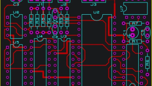
PCB layouts
2. Fundamental Principles of PCB Layouts
2.1 Component Placement Strategies
Effective component placement is the cornerstone of a successful PCB layout. Key considerations include:
- Functional Grouping: Arrange components based on their functional blocks to streamline routing and debugging processes.
- Signal Flow Optimization: Align components to facilitate a natural signal progression, minimizing trace lengths and potential interference.
- Thermal Considerations: Place heat-generating components away from sensitive circuits and incorporate thermal reliefs to manage heat dissipation.
2.2 Routing Techniques
Routing determines the path of electrical connections between components. Essential routing practices involve:
- Trace Width and Spacing: Define trace dimensions based on current-carrying requirements and voltage levels to prevent overheating and electrical arcing.
- Layer Management: Utilize multiple layers effectively, assigning specific layers for signal routing, power distribution, and grounding to reduce noise and interference.
- Via Usage: Implement vias judiciously to transition signals between layers, considering their impact on signal integrity and manufacturing complexity.
2.3 Grounding and Power Distribution
A robust grounding and power distribution strategy is vital for stable circuit operation:
- Ground Planes: Employ continuous ground planes to provide a low-impedance return path, reducing noise and EMI.
- Power Planes: Design dedicated power planes to ensure uniform voltage distribution and minimize voltage drops.
- Decoupling Capacitors: Place decoupling capacitors close to power pins of integrated circuits (ICs) to filter out noise and stabilize voltage levels.
3. Advanced PCB Layout Techniques
3.1 High-Speed Design Considerations
High-speed circuits necessitate meticulous layout practices to preserve signal integrity:
- Controlled Impedance Routing: Design traces with specific impedance values to match transmission line characteristics, minimizing reflections.
- Differential Pair Routing: Route differential signals with consistent spacing and length to ensure signal integrity and reduce EMI.
- Length Matching: Match the lengths of critical signal traces to prevent timing mismatches and data corruption.
3.2 Thermal Management in PCB Layouts
Effective thermal management ensures the reliability and longevity of electronic components:
- Thermal Vias: Incorporate thermal vias to conduct heat from hot components to larger copper areas or heat sinks.
- Copper Pours: Use copper pours to dissipate heat across the PCB surface, aiding in thermal regulation.
- Component Placement: Position heat-sensitive components away from heat sources and provide adequate spacing for airflow.
3.3 Design for Manufacturability (DFM)
Designing with manufacturability in mind streamlines production and reduces costs:
- Standardization: Adhere to standard component sizes and footprints to simplify assembly processes.
- Clearances and Tolerances: Ensure appropriate clearances between components and traces to accommodate manufacturing capabilities and tolerances.
- Test Points: Integrate test points to facilitate testing and debugging during manufacturing and maintenance.
4. PCB Layouts for Specific Applications
4.1 RF and Microwave PCB Layouts
Radio Frequency (RF) and microwave circuits require specialized layout techniques:
- Microstrip and Stripline Configurations: Utilize specific trace geometries to control impedance and signal propagation.
- Shielding: Implement shielding techniques to isolate sensitive RF circuits from external noise sources.
- Component Selection: Choose components with suitable frequency characteristics and minimize parasitic elements.
4.2 Mixed-Signal PCB Layouts
Combining analog and digital circuits necessitates careful layout strategies:
- Partitioning: Physically separate analog and digital sections to prevent noise coupling.
- Grounding Schemes: Use split or unified ground planes with proper grounding techniques to manage noise.
- Routing Practices: Avoid routing digital signals near sensitive analog traces to minimize interference.
4.3 High-Density Interconnect (HDI) PCB Layouts
HDI PCBs accommodate complex designs in compact spaces:
- Microvias: Employ microvias to connect multiple layers, enabling dense component placement.
- Sequential Lamination: Use sequential lamination processes to build up complex layer structures.
- Stacked and Staggered Vias: Implement stacked or staggered vias to optimize space and routing paths.
5. PCB Layouts and Electromagnetic Compatibility (EMC)
Ensuring electromagnetic compatibility is crucial for regulatory compliance and device performance:
- Shielding Strategies: Design enclosures and PCB shields to contain and protect against electromagnetic emissions.
- Filtering Techniques: Incorporate filters to suppress unwanted frequencies and noise.
- Layout Practices: Maintain proper spacing, grounding, and routing to minimize EMI sources.
6. Tools and Software for PCB Layouts
Modern PCB design relies on sophisticated software tools:
- Electronic Design Automation (EDA) Tools: Utilize EDA software for schematic capture, layout design, and simulation.
- Simulation and Analysis: Perform signal integrity, thermal, and electromagnetic simulations to validate designs.
- Collaboration Platforms: Leverage collaborative tools for team-based design and version control.
7. Case Studies and Practical Examples
7.1 High-Speed Processor PCB Layout
Explore the layout considerations for a high-speed processor board, focusing on signal integrity, power distribution, and thermal management.
7.2 RF Amplifier PCB Layout
Examine the design challenges and solutions in laying out an RF amplifier circuit, emphasizing impedance control and shielding.
7.3 Mixed-Signal Sensor Interface PCB Layout
Analyze the layout strategies for a mixed-signal sensor interface, highlighting partitioning and grounding techniques.
8. Common Mistakes in PCB Layouts and How to Avoid Them
Identify prevalent PCB layout errors and learn strategies to prevent them:
- Inadequate Clearance: Ensure sufficient spacing to prevent short circuits and comply with voltage ratings.
- Poor Grounding: Implement solid grounding practices to avoid noise and signal integrity issues.
- Suboptimal Component Placement: Strategically place components to facilitate routing and thermal management.
9. Future Trends in PCB Layouts
As technology advances, PCB layouts continue to evolve to meet the demands of next-generation electronic devices. Several key trends are shaping the future of PCB layouts:
9.1 Miniaturization and High-Density Interconnect (HDI) PCBs
- The growing demand for smaller, more powerful electronic devices has led to the adoption of HDI PCBs.
- Microvias, stacked vias, and buried vias are becoming more prevalent to enable complex designs in limited spaces.
- Advanced fabrication techniques such as laser drilling and sequential lamination are being used to manufacture compact and high-performance PCB layouts.
9.2 Integration of Flexible and Rigid-Flex PCB Layouts
- Flexible and rigid-flex PCBs are gaining popularity in applications such as wearables, medical devices, and aerospace electronics.
- The ability to design PCBs that can bend or fold enables more innovative product designs.
- Advanced materials, such as polyimide and liquid crystal polymer (LCP), are used to improve flexibility and durability.
9.3 AI-Driven PCB Layout Automation
- Artificial Intelligence (AI) and machine learning are being integrated into PCB design software to automate layout optimization.
- AI-driven tools can analyze signal integrity, thermal performance, and manufacturability constraints to generate optimized PCB layouts.
- This reduces design time and minimizes human errors in complex PCB layouts.
9.4 3D PCB Layouts and Embedded Components
- Traditional 2D PCB layouts are transitioning to 3D PCB designs to accommodate more functionality within a smaller footprint.
- Embedded components, such as resistors, capacitors, and ICs, are being integrated directly into PCB substrates to reduce board size and improve performance.
- 3D stacking of PCBs allows for enhanced circuit density and improved signal integrity.
9.5 Sustainable and Environmentally Friendly PCB Layout Practices
- With increasing concerns about environmental impact, PCB layout designs are adopting eco-friendly materials and manufacturing processes.
- Lead-free soldering and halogen-free laminates are being used to comply with environmental regulations such as RoHS (Restriction of Hazardous Substances).
- Recycling and disposal of PCBs are becoming key considerations in the design phase.
10. Advanced Techniques for Optimizing PCB Layouts
As electronic circuits become more complex, PCB layouts must be optimized for efficiency, reliability, and performance. The following advanced techniques can help designers create high-quality PCB layouts that meet modern design requirements.
10.1 Using Advanced Simulation Tools for PCB Layouts
- PCB design software now includes powerful simulation tools to analyze signal integrity, power distribution, and thermal performance before manufacturing.
- Tools such as SPICE, HyperLynx, and Ansys SIwave help engineers predict circuit behavior and optimize PCB layouts accordingly.
- Thermal analysis simulations ensure that heat dissipation strategies are effective, reducing the risk of overheating and component failure.
10.2 Adaptive Routing Techniques for Improved PCB Layouts
- Traditional routing methods may not be sufficient for high-speed PCBs. Adaptive routing techniques optimize trace paths to reduce noise and improve electrical performance.
- Curved Traces vs. 45-degree Angles: Curved traces reduce electromagnetic interference (EMI), making them suitable for RF and high-speed designs.
- Serpentine Routing: Used for differential pairs to match signal lengths and minimize skew in high-frequency PCB layouts.
10.3 Blind and Buried Vias for Space Optimization in PCB Layouts
- Standard through-hole vias take up valuable PCB space, limiting design flexibility.
- Blind vias connect an outer layer to an inner layer without passing through the entire board, allowing for higher component density.
- Buried vias connect inner layers without reaching the outer layers, reducing interference in high-speed designs.
- Implementing these vias improves PCB layouts for compact devices like smartphones, IoT sensors, and wearable technology.
10.4 Embedded Passives and Active Components in PCB Layouts
- Instead of mounting discrete components on the PCB surface, passive elements such as resistors and capacitors can be embedded within the PCB layers.
- Embedded components save space, reduce parasitic inductance, and improve signal integrity.
- In advanced applications, even active components like transistors and ICs can be integrated into PCB substrates, leading to more compact and efficient PCB layouts.
10.5 High-Speed Design Considerations for PCB Layouts
- High-speed PCBs require special considerations to prevent signal degradation and EMI issues.
- Controlled Impedance Routing: Ensures that signal traces maintain a consistent impedance, reducing reflections and preserving signal integrity.
- Differential Pair Routing: Used for high-speed data transmission to minimize crosstalk and signal noise.
- Minimizing Stubs: Stubs create signal reflections that degrade performance. Designers should use back-drilled vias to eliminate unnecessary via stubs in multilayer PCB layouts.
10.6 Design for Manufacturability (DFM) Strategies in PCB Layouts
- DFM principles ensure that PCB layouts are optimized for production, reducing errors and manufacturing costs.
- Minimizing Trace Width Variations: Uniform trace widths improve etching accuracy and electrical performance.
- Avoiding Acute Angles: Sharp angles in traces can lead to acid traps during etching, causing defects.
- Component Placement Optimization: Ensures ease of assembly, soldering, and rework processes.
- Solder Mask Defined (SMD) Pads vs. Non-SMD Pads: Choosing the right pad type affects the PCB assembly process and overall durability.
10.7 PCB Layouts for Multi-Board Systems
- Many electronic products require multiple interconnected PCBs, requiring careful planning of PCB layouts.
- Backplane and Daughterboard Designs: Ensuring proper signal and power distribution between multiple PCBs.
- Interconnect Design: Choosing the right connectors, flex cables, and board-to-board connections to maintain signal integrity.
- Mechanical Alignment Considerations: Using alignment holes, fiducials, and mounting points to prevent misalignment during assembly.
10.8 Impact of Material Selection on PCB Layouts
- PCB performance is significantly influenced by the choice of substrate material.
- FR4 vs. High-Frequency Materials: FR4 is commonly used for standard PCBs, while materials like Rogers, PTFE, and ceramic-based laminates are used for high-speed and RF applications.
- Thermal Conductivity Considerations: Selecting materials with high thermal conductivity improves heat dissipation in power electronics and LED applications.
- Low Dielectric Constant (Dk) Materials: Essential for maintaining consistent signal speed in high-frequency PCB layouts.
11. The Future of PCB Layouts: Emerging Technologies and Innovations
As technology advances, PCB layouts continue to evolve. Future innovations in PCB layouts are expected to enhance performance, reduce costs, and expand the possibilities for next-generation electronics.
11.1 The Rise of 3D-Printed PCB Layouts
- 3D printing technology is enabling the creation of PCBs with complex shapes and integrated components.
- Advantages of 3D-Printed PCBs:
- Customizable circuit structures.
- Reduced waste and faster prototyping.
- Integrated conductive and insulating materials.
- This technology is still in development but shows promise for advanced PCB-layouts in aerospace, medical devices, and IoT applications.
11.2 AI and Machine Learning in PCB Layouts
- AI-driven PCB-layout tools can optimize trace routing, component placement, and signal integrity analysis.
- Machine learning algorithms analyze historical design data to suggest improvements in PCB-layouts.
- AI-assisted layout tools reduce design errors, improve efficiency, and help engineers meet complex design constraints.
11.3 Integration of Optical Circuits in PCB Layouts
- Optical PCB-layouts are emerging as an alternative to traditional electrical circuits, offering higher data transmission speeds and lower power consumption.
- Benefits of Optical PCBs:
- Reduced electromagnetic interference (EMI).
- Faster data transfer for applications like data centers and high-performance computing.
- Lower power consumption compared to copper-based PCB-layouts.
11.4 Flexible Hybrid Electronics (FHE) in PCB Layouts
- Combining flexible PCB layouts with printed electronics to create lightweight, conformable circuits.
- Applications include wearable electronics, biomedical sensors, and smart textiles.
- New materials, such as stretchable conductive inks, are being developed to enhance the durability of flexible PCB layouts.
11.5 Quantum Computing and PCB Layouts
- Quantum computing circuits require specialized PCB layouts to handle cryogenic temperatures and ultra-sensitive quantum signals.
- New materials and design techniques are being explored to integrate quantum components with conventional PCB-layouts.
12. Conclusion: The Evolution of PCB Layouts
PCB-layouts are at the core of modern electronics, dictating the performance, reliability, and manufacturability of circuit boards. As electronic devices become smaller, faster, and more complex, PCB layouts must evolve to meet these challenges.
By implementing best practices in component placement, routing, and thermal management, designers can create high-quality PCB layouts that ensure optimal functionality. Advanced techniques such as HDI technology, embedded components, adaptive routing, and AI-driven design automation are pushing the boundaries of PCB layouts.
Looking ahead, emerging trends such as 3D-printed PCBs, optical circuits, and quantum computing will shape the next generation of PCB layouts. Engineers and designers must stay updated with these advancements to remain competitive in the ever-changing electronics industry.
Mastering PCB-layouts is essential for achieving high-performance, cost-effective, and manufacturable electronic products. By leveraging the latest tools, materials, and design methodologies, engineers can create cutting-edge PCB layouts that power the technology of the future.

 Quote
Quote
 E-mail