You’ve just received your PCB Gerber files, and your heart races with excitement. After all, this is the blueprint for the creation of your masterpiece: the printed circuit board that will power your product. But as you open the files, you’re hit with a question: What do all these layers mean? Which ones are essential, and how are they named in the vast landscape of Gerber files?
PCB layers are the silent architects of every electronic device, yet their names are often a mystery. If you’re designing a cutting-edge gadget, navigating the intricate language of PCB layers and Gerber files is crucial for ensuring flawless functionality. But why is the name of each layer so important? What does it say about the final product?
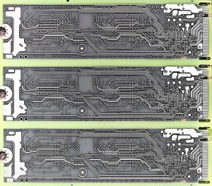
pcb layers
The truth is, the way layers are named in Gerber files impacts everything—signal flow, power distribution, manufacturing accuracy, and even the device’s overall performance. A small mistake in naming or organizing these layers can spell disaster, causing delays, malfunctions, or costly redesigns.
So, what exactly are these layers? More importantly, why does the name of each layer matter?
In this post, we’re diving deep into the world of PCB layers in Gerber files, unraveling the complexities behind their names, functions, and the significant role they play in the design-to-manufacturing process. Whether you’re an aspiring designer or a seasoned engineer, understanding these details could be the key to accelerating your PCB designs while minimizing errors.
The Importance of PCB Layers Names in Gerber Files
Imagine this: You’re in the final stages of PCB production. Your design looks flawless on the screen, but then you send it off to the manufacturer, only to discover that the board has failed basic functionality tests. The culprit? A misnamed layer in your Gerber files.
Sound far-fetched? Unfortunately, this happens more often than you’d think. Each layer in a Gerber file represents a crucial part of the PCB, from the copper traces to the solder mask to the drill holes. If one layer is improperly named or missing, the entire manufacturing process could fall apart. The wrong layer name can misdirect production, confuse fabricators, or even lead to incompatible layers being used. That’s why precise, industry-standard naming conventions aren’t just a formality—they’re a critical component of a successful PCB design.
Here’s what’s at stake:
- Signal Integrity: Layers like the copper and ground layers play pivotal roles in ensuring that signals travel seamlessly throughout the board. Mislabeling can disrupt this flow.
- Manufacturing Precision: Without proper layer naming, manufacturers might make assumptions that compromise the board’s structural and electrical integrity.
- Production Efficiency: Miscommunication or errors in layer definition can lead to delays, costing both time and money.
The Key Layers in a PCB Gerber File and Their Names
Understanding the names of PCB layers in a Gerber file is like learning a secret code. Every layer has a specific purpose, and the way it’s named reveals crucial information to both designers and manufacturers. Let’s break down the most common layer names in Gerber files.
1. Copper Layers (GTL, GBL, etc.)
At the heart of your PCB, copper layers are the powerhouses. These layers form the intricate pathways through which electrical signals flow, powering your device. In Gerber files, they are usually named GTL (Top Layer) for the upper side of the PCB and GBL (Bottom Layer) for the lower side. Some designs feature inner layers, which may be labeled G1, G2, etc.
- Top Layer (GTL): This is where the primary electrical components are placed. The traces that interconnect components on the top side of the PCB are etched into this layer.
- Bottom Layer (GBL): This layer contains traces that connect the components placed on the bottom side of the PCB.
- Inner Layers (G1, G2, etc.): These layers are used in multi-layer boards. They handle additional signal traces, power planes, and ground planes. Proper naming here is crucial for avoiding short circuits and interference.
2. Solder Mask Layer (SMT, SMO, etc.)
The solder mask is a protective layer that prevents unwanted connections and short circuits during soldering. It’s applied over the copper layers, leaving only the copper pads exposed. The solder mask ensures that solder only flows where it’s supposed to.
- Top Solder Mask (SMT): This layer corresponds to the solder mask that covers the top copper layer.
- Bottom Solder Mask (SMO): Likewise, this layer covers the bottom copper layer, protecting the traces on the underside of the PCB.
3. Silkscreen Layer (GTO, GBO, etc.)
Imagine your PCB as a miniature city. Just like a city needs signs, roads, and labels to guide its inhabitants, your PCB needs a silkscreen layer. The silkscreen layer contains markings for component placement, logos, and labels—essentially the “blueprint” that tells assemblers where to place each component.
- Top Silkscreen (GTO): This marks the labels, logos, and component positions on the top of the PCB.
- Bottom Silkscreen (GBO): Similarly, this marks the silkscreen on the bottom side of the PCB.
4. Drill Layer (X-Y Drill, etc.)
Drill layers are perhaps the most crucial for multi-layer PCBs. These layers define the location and size of all holes that will be drilled into the board. Whether the holes are for through-hole components or vias (connections between layers), the drill layer ensures that every hole is positioned correctly.
- Drill File (X-Y Drill): A drill file outlines the exact coordinates where the holes should be drilled. In multi-layer boards, vias will be used to interconnect the various layers of the PCB.
5. Paste Mask Layer (PST, PSO, etc.)
In soldering, the paste mask layer controls where solder paste is applied. This layer ensures that only the pads for the components are coated with solder paste, allowing for precise assembly during the surface mount process.
- Top Paste Mask (PST): Used for controlling solder paste placement on the top side of the PCB.
- Bottom Paste Mask (PSO): Controls solder paste application on the bottom side.
Why Proper Layer Naming Is Vital for the Manufacturing Process
Gerber files are the bridge between design and manufacturing. They carry all the information a PCB manufacturer needs to create a functional product—everything from trace width to drill hole size to the copper layer alignment. But if the layers aren’t properly named, the manufacturer can end up with a lot of confusion.
- Efficiency and Accuracy: Misnamed or misrepresented layers can lead to unnecessary production delays. Incorrect copper layers could mean the PCB gets routed the wrong way, or the silkscreen might end up misaligned with the components.
- Signal Integrity: The layers in Gerber files affect how well your device will function. If the naming of power or ground layers is off, you might end up with noisy circuits or worse—components that just won’t work as expected.
- Cost Savings: A small mistake in naming can snowball into a large issue that could result in scrapped boards or rework. Properly named layers make the entire process smoother, cutting down on manufacturing costs and time.
Conclusion: The Power of Properly Named PCB Layers in Gerber Files
In the world of PCB design, layer naming might seem like a small detail, but it’s anything but. It’s the unsung hero that determines whether your design will succeed or fail. Understanding the names and functions of each layer in a Gerber file ensures that your PCB will be functional, efficient, and manufacturable. So the next time you’re working with Gerber files, take a moment to appreciate the subtle power of each layer’s name. It could be the difference between an elegant design and a costly mistake.
Understanding the PCB layers name in Gerber files is more than just an industry convention; it’s a pathway to creating devices that are precise, reliable, and ready for the market. With proper layer names, you’re setting the foundation for a high-quality, high-performance PCB.
our linken sqpcb.com

- long board pcb
- Flexible PCBs
- Special PCB
- Express Printed Circuit Board
- Pcb Prototype
- LED PCB
- PCB
- Printed Circuit Board
- Pcb meaning
- Pcb manufacturer
- Rigid pcb board
- Rigid Flex PCB
 Quote
Quote
 E-mail