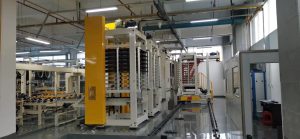
PCB Lamination Process: Key Techniques and Best Practices In PCB Manufacturing
Introduction
Lamination is a critical process in PCB (Printed Circuit Board) manufacturing, where multiple layers of copper and dielectric materials are bonded together under high temperature and pressure to form a multilayer PCB. The lamination process ensures electrical insulation, mechanical strength, and structural integrity of the final circuit board.
As PCB designs become increasingly complex and high-density, ensuring proper lamination is essential to prevent delamination, warping, resin voids, and electrical failures. This article explores the PCB lamination process, key factors affecting lamination quality, material selection, and process optimization techniques to achieve high-reliability multilayer PCBs.

PCB Lamination Process
The PCB Lamination Process Step by Step
1. Material Preparation
Before lamination, all PCB layers must be clean, properly aligned, and ready for bonding. The key materials involved include:
- Copper Foil: Conductive layer for PCB circuits.
- Prepreg (PP): Semi-cured resin that acts as the adhesive between PCB layers.
- Core Layers: Pre-manufactured inner layers with circuit patterns.
- Release Films & Buffer Materials: Prevent contamination and ensure uniform pressure distribution.
2. Stack-Up and Alignment
- Inner and outer layers are stacked with prepreg in between, following a designed stack-up structure.
- Precise alignment is crucial to ensure accurate registration of circuit traces.
- Pinning systems or optical alignment tools help prevent shifting during lamination.
3. Pre-Pressing (Tack Lamination)
- A low-pressure pre-press step helps hold layers together before full lamination.
- This prevents layer shifting and misalignment during transfer to the main press.
- Pre-pressing also removes trapped air, reducing the risk of voids and bubbles.
4. High-Pressure & High-Temperature Lamination
- The stack is placed into a hydraulic or vacuum press, applying:
- Heat (130°C – 200°C): Allows prepreg resin to flow and bond layers.
- Pressure (200 – 400 psi): Ensures full adhesion and eliminates air gaps.
- Time (30 – 90 minutes): Ensures complete resin curing and mechanical stability.
- The controlled heating and pressure cycles prevent resin starvation, delamination, and stress build-up.
5. Cooling and Cold Pressing
- After heat lamination, gradual cooling is essential to prevent stress-related defects.
- A cold press step helps stabilize resin bonding and minimize internal stress.
- Rapid cooling or uneven cooling can cause warping and cracking.
6. Post-Lamination Inspection and Processing
- Thickness measurement ensures the laminated PCB meets specifications.
- X-ray or optical inspection checks for layer misalignment or voids.
- The laminated panel then proceeds to drilling, plating, and further processing.
Key Factors Affecting Lamination Quality
1. Stack-Up Symmetry
- A symmetrical stack-up minimizes stress differences and prevents board warping.
- Uneven prepreg thickness or copper weight leads to expansion mismatches, increasing the risk of deformation.
2. Prepreg Selection & Resin Flow Control
- The prepreg type and resin content must match copper thickness and layer count.
- Low resin flow can lead to voids and weak adhesion, while excessive resin flow may cause over-compression and electrical performance issues.
- Thicker copper layers require high-flow prepreg to ensure full bonding.
3. Lamination Temperature and Pressure Control
- Gradual heating and controlled pressure application help ensure uniform resin flow.
- Sudden temperature changes can cause uneven curing and stress build-up, leading to delamination or layer separation.
4. Cooling Rate and Cold Pressing
- Rapid cooling can introduce internal stress, causing PCBs to warp or crack.
- A controlled cold press cycle stabilizes the board and maintains dimensional accuracy.
5. Copper Balance and Residual Stress Management
- Uneven copper distribution leads to expansion differences, which can warp the board.
- Copper balancing techniques should be applied in design to reduce lamination stress.
6. Cleanroom and Contamination Control
- Dust, oil, or moisture can cause lamination defects like voids and resin contamination.
- Lamination should take place in a cleanroom environment to prevent contamination.
Common Lamination Defects and How to Prevent Them
| Defect | Cause | Prevention |
|---|---|---|
| Delamination | Incomplete resin curing, contamination, poor adhesion | Optimize heating cycles, use clean materials, ensure full resin flow |
| Resin Voids | Air trapped during lamination | Pre-press layers, use vacuum lamination, ensure proper pressure |
| Board Warping | Asymmetrical stack-up, uneven cooling | Use symmetrical layers, controlled cooling, and cold pressing |
| Layer Misalignment | Improper stack alignment, shifting during lamination | Use alignment pins, optical alignment, and pre-pressing |
| Thickness Variation | Uneven resin flow, excessive pressure | Control resin content, optimize pressing parameters |
Best Practices for High-Quality PCB Lamination
- Use a well-balanced and symmetrical stack-up to prevent warping.
- Select prepreg with the right resin content based on copper weight and layer count.
- Optimize lamination temperature, pressure, and time to ensure complete resin curing.
- Implement a cold press cycle to minimize internal stress and improve stability.
- Monitor copper balance and stress distribution in PCB design to reduce expansion mismatches.
- Maintain a clean environment to prevent contamination-related defects.
- Regularly inspect laminated panels using X-ray or optical testing to ensure quality.
Conclusion
Lamination is a critical step in multilayer PCB manufacturing, directly impacting board reliability, structural integrity, and electrical performance. By optimizing stack-up design, resin flow, heat and pressure control, and cooling techniques, manufacturers can achieve high-quality lamination results and prevent defects like delamination, warping, and resin voids.
Implementing best practices and strict process controls ensures that laminated PCBs meet the performance and durability requirements for high-speed, high-frequency, and HDI applications. As PCB technology advances, continuous improvements in lamination techniques and materials will further enhance manufacturing efficiency and product reliability.
- long board pcb
- Flexible PCBs
- Special PCB
- Express Printed Circuit Board
- Pcb Prototype
- LED PCB
- PCB
- Printed Circuit Board
- Pcb meaning
- Pcb manufacturer
- Rigid pcb board
- Rigid Flex PCB

 Quote
Quote
 E-mail