PCB electrical testing
PCB Electrical Testing
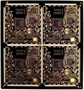
Electrical testing ensures that the circuits on the PCB function correctly and that there are no open circuits, short circuits, or other electrical anomalies. This testing is vital for verifying the integrity of conductive paths, component placement, and functionality.
AOI (Automated Optical Inspection)
AOI employs high-resolution cameras and advanced imaging software to inspect PCBs for defects during manufacturing. This automated approach is critical for maintaining quality in fast-paced production environments.
Key Features
- Defect Detection: Identifies surface defects, component misplacement, missing parts, and solder joint issues with exceptional precision.
- Versatility: Suitable for various PCB designs, from high-density fine-pitch boards to low-density, large-sized boards.
- Efficiency: Enhances production efficiency by catching defects early in the assembly process.
Advantages
- Reduced Costs: Early defect detection minimizes repair costs and prevents faulty boards from advancing to later stages.
- Improved Yield: Avoids passing defective boards to subsequent stages, improving overall product yield.
- Process Control: Ensures consistent welding quality and tighter control of assembly processes, reducing variability.
Applications
- High-Volume Production: Ideal for large-scale manufacturing, ensuring consistent quality.
- Early-Stage Quality Control: Essential for complex assembly processes where early intervention can prevent downstream failures.
- Automotive and Medical PCBs: AOI excels in industries where precision and reliability are paramount.
PCB Electrical Testing:Test Fixture Test
The test fixture method relies on custom-designed mechanical setups to test the functionality and reliability of PCBs. This method is particularly effective for high-volume production where repeatability is critical.
Main Components
- Fixture Frame: Provides the primary structure and support for the testing setup.
- Needle Plate: Houses numerous test probes to make precise electrical contact with the PCB.
- Carrier Plate: Positions and secures the PCB for accurate alignment during testing.
- Pressing Plate: Features pressing bars to apply consistent pressure for stable contact.
- Pressing Mechanism: Includes quick clamps and a guide system for controlled movement of the pressing plate.
Advantages
- High Precision: Delivers accurate and reliable results, especially for densely populated PCBs with complex layouts.
- Cost-Effective Maintenance: Modular design reduces downtime and maintenance costs while allowing for easy upgrades.
- Scalability: Highly efficient for large-scale testing of standardized PCB designs.
Applications
- Mass Production: Ideal for testing standardized PCBs in large quantities.
- Repetitive Testing Needs: Ensures accuracy and repeatability in high-volume manufacturing.
- Consumer Electronics: Common in testing boards for appliances, smartphones, and similar products.
PCB Electrical Testing:Flying Probe Test
The flying probe test is a versatile and cost-effective solution for testing small batches, prototypes, or complex PCBs. It uses high-speed movable probes to contact specific points on the PCB, eliminating the need for costly test fixtures.
Working Principle
- Dynamic Probes: High-speed probes move along the X-Y axis to contact PCB pads and vias.
- Signal Testing: Sensors and drivers measure electrical characteristics such as continuity, resistance, and component values.
- Defect Identification: Cameras detect missing components, polarity issues, and solder defects with precision.
Key Features
- Precision: Supports a minimum test gap of 0.2 mm, making it suitable for high-density designs.
- High Accuracy: Probe positioning accuracy reaches 5-15 μm, ensuring reliable test results.
- Non-Destructive Testing: Protects the PCB from damage during the testing process.
Advantages
- Cost Savings: Eliminates the need for custom test fixtures, reducing setup costs.
- Rapid Prototyping: Shortens the development cycle, enabling faster time-to-market for new products.
- Flexibility: Adapts to different designs, making it ideal for custom PCBs and low-volume production.
Applications
- Prototype Testing: Evaluates functionality and reliability during the design phase.
- Custom PCB Production: Suitable for unique or specialized PCB designs.
- High-Density Boards: Effective for testing boards with compact layouts and fine-pitch components.
PCB Electrical Testing:Additional Testing Methods
Boundary Scan Testing
- Embedded within ICs, this method tests interconnections and identifies faults in multi-layer or complex boards.
ICT (In-Circuit Testing)
- Directly applies electrical signals to individual components, detecting solder defects, missing parts, and electrical anomalies.
X-Ray Inspection
- A non-destructive method for identifying internal defects like solder voids or misaligned components, especially in BGA and QFN packages.
Functional Testing
- Simulates the PCB’s real-world operational environment to verify its overall functionality.
Emerging Trends in PCB Testing
Advanced Automation
- Integration of AI and machine learning to improve defect detection and streamline processes.
- Automated systems reducing human intervention and boosting testing efficiency.
High-Frequency Testing
- Ensures signal integrity for high-speed communication systems by testing for issues like signal loss, crosstalk, and impedance mismatches.
Eco-Friendly Testing Methods
- Adoption of sustainable practices, including reusable test fixtures and energy-efficient equipment.
- Development of recyclable materials to align with green manufacturing goals.
Conclusion
Electrical testing is a cornerstone of PCB production, ensuring that every board meets stringent quality and performance standards. From the precision of flying probe testing to the efficiency of automated optical inspection, each method contributes to creating reliable, high-quality PCBs. By leveraging advanced testing techniques and embracing emerging trends, manufacturers can continue to innovate while delivering flawless products to the market.
our linken sqpcb.com

- long board pcb
- Flexible PCBs
- Special PCB
- Express Printed Circuit Board
- Pcb Prototype
- LED PCB
- PCB
- Printed Circuit Board
- Pcb meaning
- Pcb manufacturer
- Rigid pcb board
- Rigid Flex PCB
 Quote
Quote
 E-mail