Minimum Solder Mask Sliver: Importance, Standards, and Design Considerations
1. Introduction to Solder Mask Sliver
Solder mask sliver refers to the narrowest width of solder mask material between adjacent copper traces or pads on a printed circuit board (PCB). It plays a crucial role in preventing short circuits, solder bridging, and oxidation, ensuring the reliability of the PCB.
As PCBs become more compact and high-density, the challenge of maintaining a proper solder mask sliver width increases. If the sliver is too narrow, it may peel off, break, or cause manufacturing defects. Conversely, excessive spacing can lead to unintended solder connections.
In this article, we will explore minimum solder mask sliver requirements, industry standards, design considerations, and manufacturing challenges to help PCB designers optimize their layouts for high reliability.
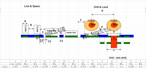
minimum solder mask sliver
2. Understanding Minimum Solder Mask Sliver
The minimum solder mask sliver is the narrowest spacing of solder mask between conductive features, such as traces, pads, and vias. It ensures electrical isolation and protection from contamination, moisture, and mechanical damage.
2.1 Why is Solder Mask Sliver Important?
✅ Prevents Solder Bridging – Reduces the risk of unintended electrical connections during soldering.
✅ Enhances Electrical Isolation – Provides insulation between closely spaced copper features.
✅ Improves PCB Durability – Protects circuits from corrosion, dust, and moisture.
✅ Affects Manufacturing Yield – A well-designed sliver minimizes production defects and rework costs.
3. Industry Standards for Minimum Solder Mask Sliver
The minimum acceptable solder mask sliver depends on manufacturing capabilities and industry standards. The most widely referenced standard is IPC-6012 (Qualification and Performance Specification for Rigid PCBs), which provides guidelines for PCB designers and manufacturers.
3.1 IPC Standards for Solder Mask Sliver
| PCB Class | Typical Minimum Solder Mask Sliver | Application |
|---|---|---|
| Class 1 | ≥ 4 mil (0.10 mm) | Consumer electronics, low-reliability applications |
| Class 2 | ≥ 3 mil (0.075 mm) | Industrial, automotive, and general applications |
| Class 3 | ≥ 2 mil (0.05 mm) | High-reliability, aerospace, medical PCBs |
- Class 1 PCBs have the most relaxed tolerances, suitable for low-cost consumer products.
- Class 2 PCBs require tighter control, commonly used in industrial and automotive applications.
- Class 3 PCBs demand the highest precision, used in mission-critical electronics.
3.2 Manufacturer Limitations
Modern PCB manufacturers typically offer minimum solder mask sliver widths of 2–3 mils (0.05–0.075 mm), but achieving such fine spacing depends on:
✅ Advanced lithography and solder mask application processes
✅ Precise alignment of solder mask layers
✅ Controlled PCB manufacturing tolerances
4. Design Considerations for Minimum Solder Mask Sliver
4.1 Solder Mask Type Selection
The type of solder mask used affects the minimum achievable sliver width. Common types include:
🔹 Liquid Photoimageable (LPI) Solder Mask – Most widely used, allowing for fine features.
🔹 Dry Film Solder Mask – Suitable for high-precision applications but more expensive.
🔹 Inkjet-Printed Solder Mask – Used for prototypes and small-scale production.
LPI solder mask is the industry standard, supporting minimum slivers down to 2 mil (0.05 mm) in advanced PCB manufacturing.
4.2 Copper Trace Spacing and Pad Layout
To avoid excessively small solder mask slivers, designers should:
✅ Increase pad-to-pad spacing – Allows for a wider solder mask between features.
✅ Use solder mask-defined pads (SMD pads) – Ensures mask coverage over the pad edges.
✅ Avoid over-constraining design rules – Work within manufacturer capabilities.
4.3 Alignment Tolerance in Manufacturing
During PCB fabrication, solder mask alignment tolerance must be considered. A mask shift of ±2–3 mils (0.05–0.075 mm) is common, so designers should:
✅ Leave extra clearance around critical areas
✅ Check with the PCB manufacturer for specific alignment tolerances
✅ Use design rule checks (DRC) in PCB software
5. Common Challenges with Minimum Solder Mask Sliver
5.1 Solder Mask Peeling or Lifting
🔸 If the solder mask sliver is too thin, it may detach during soldering or PCB handling.
🔸 Solution: Increase sliver width where possible or use alternative mask types.
5.2 Solder Bridging
🔸 Insufficient solder mask sliver can result in solder bridges between pads or traces.
🔸 Solution: Increase spacing between pads or use non-solder mask defined (NSMD) pads.
5.3 Manufacturing Yield Issues
🔸 Small solder mask slivers are difficult to fabricate, leading to higher rejection rates.
🔸 Solution: Balance fine-pitch designs with manufacturable tolerances.
6. How to Optimize PCB Design for Solder Mask Sliver
To ensure a reliable and manufacturable PCB, follow these best practices:
✅ Follow Manufacturer Design Guidelines – Every PCB fabricator has different process capabilities.
✅ Set Proper Design Rule Checks (DRC) – Define minimum solder mask sliver limits in PCB software.
✅ Use Solder Mask-Defined Pads (SMDs) When Necessary – Helps control solder mask registration.
✅ Minimize Fine-Pitch Components When Possible – Reduces the risk of mask misalignment issues.
✅ Request DFM Feedback from the PCB Manufacturer – Ensures design feasibility before production.
7. Future Trends in Solder Mask Design
With the rise of miniaturization and high-density PCB designs, new technologies are emerging to address solder mask challenges:
🔹 Improved Lithography Techniques – Allow for finer mask definitions.
🔹 Advanced Solder Mask Materials – Provide better adhesion and durability.
🔹 Automated Optical Inspection (AOI) – Ensures precision in mask application.
🔹 Inkjet Solder Mask Printing – Enables on-demand mask application with tighter tolerances.
These advancements will push the limits of minimum solder mask sliver while maintaining high reliability and manufacturability.
8. Conclusion: Ensuring Optimal Solder Mask Sliver in PCB Design
The minimum solder mask sliver plays a vital role in PCB reliability, soldering performance, and electrical insulation. To achieve an optimal design:
🔹 Follow IPC-6012 standards for minimum solder mask sliver requirements.
🔹 Work within manufacturing tolerances to prevent misalignment and defects.
🔹 Optimize PCB layout to avoid excessively thin solder mask slivers.
🔹 Consult with PCB manufacturers to ensure design-for-manufacturability (DFM) compliance.
For high-quality PCB fabrication, Shenzhen Shuoqiang Electronics offers precision manufacturing and expert design guidance to help engineers achieve optimal solder mask performance in advanced circuit boards.
our linkedin sqpcb.com

- long board pcb
- Flexible PCBs
- Special PCB
- Express Printed Circuit Board
- Pcb Prototype
- LED PCB
- PCB
- Printed Circuit Board
- Pcb meaning
- Pcb manufacturer
- Rigid pcb board
- Rigid Flex PCB
 Quote
Quote
 E-mail