Introduction
The evolution of electronic devices has led to increasingly complex and miniaturized printed circuit boards (PCBs). To meet the demands of high-density interconnects (HDI) and multilayered designs, advanced drilling techniques are essential. Laser drill technology has emerged as a pivotal method in PCB manufacturing, offering precision, efficiency, and adaptability that traditional mechanical drilling methods struggle to match. This article delves into the intricacies of laser drill technology, exploring its principles, applications, advantages, and future prospects in the realm of PCB fabrication.
1. Fundamentals of Laser Drill Technology in PCB Manufacturing
1.1 Principles of Laser Drilling
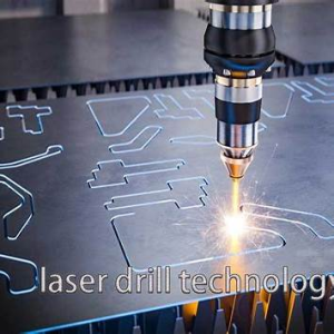
Laser drilling utilizes concentrated light energy to ablate material from the PCB substrate, creating vias and holes without physical contact. This non-mechanical approach allows for high precision and minimal damage to surrounding areas.
1.2 Types of Lasers Used
Different laser sources are employed based on the material and desired hole characteristics:
-
CO₂ Lasers: Ideal for drilling through organic materials like FR-4 due to their longer wavelengths.
-
UV Lasers: Suitable for fine-feature drilling, offering higher absorption in a variety of materials.
1.3 Comparison with Mechanical Drilling
Unlike mechanical drilling, which uses physical bits, laser drilling offers:
-
Higher precision and smaller hole diameters.
-
Reduced mechanical stress on the PCB.
-
Faster processing times for complex patterns.
Laser drill technology
2. Applications of Laser Drill Technology in PCB Manufacturing
2.1 Microvias and HDI PCBs
Laser drilling is instrumental in creating microvias, essential for HDI PCBs, enabling higher circuit density and improved electrical performance.
2.2 Blind and Buried Vias
The technology facilitates the creation of blind and buried vias, connecting different layers without penetrating the entire board, thus saving space and enhancing functionality.
2.3 Flexible and Rigid-Flex PCBs
In flexible and rigid-flex PCBs, laser drilling ensures precise hole placement without damaging delicate substrates, crucial for wearable and compact devices.
3. Advantages of Laser Drill Technology in PCB Manufacturing
3.1 Precision and Accuracy
Laser drilling achieves hole diameters as small as 20 micrometers with high positional accuracy, essential for modern miniaturized electronics.
3.2 Non-Contact Process
The non-contact nature eliminates tool wear and reduces the risk of substrate damage, enhancing the longevity and reliability of PCBs.
3.3 Versatility
Capable of drilling various materials and complex geometries, laser drilling adapts to diverse PCB designs and requirements.
4. Challenges and Considerations in Laser Drill Technology
4.1 Thermal Effects
Excessive heat can cause delamination or damage to adjacent areas. Proper parameter settings and cooling mechanisms are vital to mitigate thermal issues.
4.2 Material Compatibility
Different substrates absorb laser energy differently. Understanding material properties ensures optimal drilling outcomes.
4.3 Equipment Costs
Initial investment in laser drilling equipment is significant. However, the long-term benefits often justify the expenditure.
5. Future Prospects of Laser Drill Technology in PCB Manufacturing
5.1 Integration with Automation
Combining laser drilling with automated systems enhances throughput and consistency, meeting the demands of mass production.
5.2 Advancements in Laser Technology
Developments in ultrafast and fiber lasers promise even greater precision and efficiency in PCB drilling applications.
5.3 Sustainable Manufacturing
Laser drilling contributes to greener manufacturing by reducing waste and eliminating the need for consumables like drill bits.
5.4 Integration with AI and Smart Manufacturing
One of the most promising directions for Laser Drill Technology in PCB manufacturing is its integration with artificial intelligence (AI) and machine learning (ML) systems. These advanced systems enable predictive maintenance, adaptive control of drilling parameters, and real-time quality assurance. In the context of smart factories, Laser Drill Technology can be embedded in a closed-loop system where performance is constantly analyzed, and adjustments are automatically made to ensure optimal outcomes.
The AI-driven Laser Drill Technology platform might also enable predictive analytics to determine tool life, detect wear patterns in optics or laser sources, and forecast potential breakdowns before they happen. This approach minimizes downtime and enhances equipment efficiency, all while maintaining the high precision that Laser Drill Technology is known for.
5.5 Nanosecond and Picosecond Lasers for Enhanced Resolution
The development of ultrafast laser systems—such as nanosecond, picosecond, and femtosecond lasers—presents a major leap forward for Laser Drill Technology. These systems deliver extremely short pulses of energy, reducing the heat-affected zone (HAZ) and thereby improving the integrity of the drilled holes.
Picosecond and femtosecond lasers are particularly suitable for applications where extremely fine resolution is necessary, such as in medical or aerospace PCBs. With these lasers, Laser Drill Technology can drill features that were once impossible or required costly post-processing. As these laser systems become more cost-effective, their use will likely become standard in advanced PCB fabrication.
5.6 Hybrid Drilling Systems
Future developments may also lead to more widespread use of hybrid drilling systems that combine mechanical and Laser Drill Technology into a single platform. Such systems can utilize the strengths of both methods: laser drilling for precision microvias and mechanical drilling for larger or through-hole vias.
This hybrid approach can enhance manufacturing flexibility while streamlining equipment investment and factory footprint. Manufacturers that need to produce a broad range of PCBs—from conventional double-layer boards to HDI multilayer structures—will particularly benefit from these all-in-one systems.
5.7 Environmental Considerations and Sustainable Engineering
Environmental sustainability is becoming increasingly vital across all industries, including electronics manufacturing. Laser Drill Technology has several environmentally favorable attributes, such as the elimination of drill bit waste and reduced use of lubricants or cutting fluids common in mechanical drilling.
In the coming years, manufacturers are likely to adopt more energy-efficient laser systems and refine processes to further reduce emissions, energy usage, and material waste. The shift to greener laser-based PCB drilling processes aligns with global sustainability initiatives and emerging regulatory pressures, especially in Europe and North America.
Additionally, Laser Drill Technology’s contactless nature means that it produces less particulate contamination, improving air quality in the factory environment and reducing the burden on filtration systems. New technologies such as dry or low-dust ablation will further reinforce Laser Drill Technology’s environmentally responsible profile.
6. Quality Control and Inspection Methods for Laser Drill Technology in PCB Manufacturing
6.1 In-Line Optical Inspection
Quality assurance is critical in any high-precision manufacturing process. Laser Drill Technology necessitates highly sensitive inspection systems to detect defects such as misalignment, incomplete vias, and surface scorching. In-line optical inspection (AOI) systems are commonly used immediately following the laser drilling process to catch defects in real time.
Advanced AOI systems are now integrated with AI algorithms to interpret visual data and distinguish between acceptable and defective patterns. These systems can also communicate with the Laser Drill Technology platform, prompting real-time corrections and reducing waste.
6.2 Cross-Section Analysis
Though time-consuming and often used for batch sampling rather than continuous production, cross-section analysis remains an essential method for validating hole geometry, depth, taper, and layer alignment. Cross-sectional views provide a clear picture of the internal structure of microvias or blind vias produced by Laser Drill Technology, confirming that the drill process has maintained the required specifications.
6.3 X-Ray Inspection and CT Scanning
For multilayer PCBs, X-ray inspection can be used to assess the accuracy of stacked via alignments and to detect any internal bridging or delamination caused during laser drilling. With modern 3D CT scanning, manufacturers can obtain volumetric models of the PCB, allowing in-depth inspection without destroying the product.
These tools are invaluable in ensuring that Laser Drill Technology not only meets design tolerances but also complies with industry standards such as IPC-6012 for rigid PCBs and IPC-2226 for HDI structures.
7. Industry Standards and Certification for Laser Drill Technology in PCB Manufacturing
7.1 IPC Standards Related to Laser Drilling
The Institute for Printed Circuits (IPC) provides numerous standards related to laser drilling, especially for HDI and microvia PCBs. IPC-6012, IPC-6016 (for HDI boards), and IPC-2221 cover the acceptability and design aspects of laser-drilled vias. These standards ensure consistency across manufacturers and help in qualifying Laser Drill Technology for both commercial and critical applications.
7.2 ISO and UL Compliance
Laser Drill Technology equipment and processes often must comply with global quality and safety standards such as ISO 9001 (Quality Management Systems), ISO 14001 (Environmental Management), and UL recognition for flammability and material safety.
Meeting these requirements not only ensures product quality but also enhances market acceptance, particularly in aerospace, automotive, and medical sectors where compliance is mandatory.
8. Case Studies: Successful Implementation of Laser Drill Technology in PCB Manufacturing
8.1 Case Study 1: Smartphone HDI PCB Production
A leading mobile phone manufacturer adopted CO₂ and UV-based Laser Drill Technology to increase its production yield for HDI smartphone PCBs. The result was a 30% reduction in via failure rates and a 25% increase in throughput due to the elimination of tool changeovers and the adoption of inline quality control.
8.2 Case Study 2: Automotive Control Systems
In the automotive industry, precision and reliability are non-negotiable. A Tier-1 supplier implemented picosecond Laser Drill Technology to create microvias in safety-critical electronic control units (ECUs). These microvias reduced the board size by 20%, enabling more compact designs without sacrificing reliability.
8.3 Case Study 3: Medical Device Implantable Sensors
An implantable glucose sensor manufacturer required laser-drilled holes with extreme precision and minimal thermal impact. Laser Drill Technology using femtosecond lasers allowed drilling of biocompatible materials like polyimide with high aspect ratio and zero carbonization—something mechanical drilling could not achieve.
9. Training and Workforce Development for Laser Drill Technology
9.1 Skill Requirements
Laser Drill Technology requires operators who understand optics, material science, and digital manufacturing. As the complexity of PCBs grows, so too does the need for highly trained technicians and engineers capable of operating and maintaining sophisticated laser systems.
9.2 In-House vs. Outsourced Training
Some manufacturers develop in-house training programs specific to their equipment and workflows. Others rely on OEMs or third-party institutions for certified training in Laser Drill Technology.
As automation grows, continuous education in digital monitoring, programming, and maintenance will be necessary to stay competitive in the industry.
10. Conclusion: The Future Is Laser-Driven
Laser Drill Technology is no longer an emerging option; it is a cornerstone of modern PCB manufacturing. From consumer electronics to mission-critical aerospace systems, the ability to drill with micron-level precision, at high speed, with minimal waste, sets Laser Drill Technology apart from traditional methods.
As laser systems become more intelligent, energy-efficient, and precise, their role in PCB manufacturing will expand further—enabling more compact devices, greater functionality, and higher production yields. Companies investing in Laser Drill Technology today are setting the foundation for tomorrow’s innovations.
As the landscape of printed circuit board (PCB) manufacturing evolves at an unprecedented pace, driven by miniaturization, high-density designs, and the rise of 5G, AI, and IoT applications, the role of Laser Drill Technology becomes more central than ever. The technology, once considered an auxiliary or specialized process, has matured into a transformative capability, enabling the production of complex multilayer, HDI, and rigid-flex boards with unmatched precision and speed.
However, to truly understand the long-term significance of Laser Drill Technology, it is essential to evaluate not just its current impact but also the broader trajectory it offers to the electronics industry. The conclusion of this discussion goes beyond summarizing facts—it seeks to highlight how laser drilling redefines boundaries, integrates with evolving digital ecosystems, and catalyzes innovation for decades to come.
1. The Strategic Value of Laser Drill Technology in a Competitive Landscape
In today’s hyper-competitive electronics market, speed-to-market, design flexibility, and manufacturing efficiency are essential. Laser Drill Technology meets all these imperatives. Its non-contact, highly accurate nature significantly reduces mechanical stress on substrates, offering superior yield rates and reducing rework.
While traditional mechanical drilling remains suitable for certain through-hole and low-precision applications, it falls short in addressing the demands of HDI, microvia, and sub-100 μm via structures. The strategic adoption of Laser Drill Technology thus becomes not merely a technological upgrade, but a necessary evolution for manufacturers looking to stay relevant in next-generation PCB production.
2. From Precision to Perfection: Reproducibility and Yield Benefits
One of the most significant advantages of laser drilling is its reproducibility. Unlike mechanical tools that wear over time, resulting in drift and inconsistency, laser systems deliver consistent pulse energy and beam quality over long durations. This consistency directly translates into higher yields and fewer defects—particularly important in industries like aerospace, automotive, and healthcare where reliability is paramount.
Additionally, the reduced need for frequent tool changes, lower maintenance, and elimination of physical drill bits enhances uptime and throughput. When paired with automated inspection systems and real-time process feedback, Laser Drill Technology empowers manufacturers to achieve near-zero-defect production—a vision that once seemed idealistic.
3. The Expanding Role of Laser Drill Technology in Emerging Applications
With the rise of wearable tech, implantable medical devices, automotive ADAS systems, and flexible electronics, PCBs are being integrated into new form factors and subjected to diverse operational environments. These applications require ultra-thin boards, ultra-small vias, and unconventional materials—all of which benefit immensely from the capabilities of Laser Drill Technology.
In wearable and implantable electronics, for example, bio-compatible materials like polyimide or LCP (liquid crystal polymer) must be drilled with exceptional precision while minimizing thermal damage. In automotive control systems, the need for high-speed signal integrity demands microvias with excellent copper-to-substrate adhesion, for which laser ablation offers ideal results.
4. Environmental Sustainability and Laser Drill Technology
Sustainability is no longer an afterthought in manufacturing. Stakeholders across the supply chain are re-evaluating processes based on their carbon footprint, energy consumption, and waste generation. Laser Drill Technology, with its contactless operation and minimal mechanical wear, contributes positively to this shift.
Notably, it reduces reliance on consumables like drill bits, cutting fluids, and coolant chemicals, thereby lowering material waste. Furthermore, advances in solid-state and diode-pumped lasers are making high-efficiency, low-power-consumption systems increasingly viable for mainstream manufacturing.
Manufacturers investing in greener production methods will find that Laser Drill Technology offers not just technical benefits, but also strategic alignment with global environmental directives like RoHS, REACH, and the European Green Deal.
5. Bridging the Talent and Training Gap
As laser-based systems become more prevalent, the demand for skilled operators, technicians, and engineers who can program, maintain, and optimize them will rise in parallel. The knowledge base required to fully harness Laser Drill Technology spans optics, thermodynamics, digital controls, and materials science.
Addressing this challenge means investing in workforce development—through academic collaboration, industry certification, and continuous in-house training. Companies that cultivate such talent pipelines will not only operate laser systems more effectively but will also gain a competitive edge through process innovation and rapid troubleshooting.
6. Challenges and Barriers to Broader Adoption
Despite its many advantages, Laser Drill Technology is not without challenges. Initial capital expenditure remains a significant barrier for smaller manufacturers. Additionally, the learning curve associated with process tuning, laser safety management, and system integration can deter adoption.
In certain cases, laser-drilled vias may require additional post-processing steps, such as desmearing or conductive seed layer deposition, to achieve optimal plating characteristics. Moreover, achieving tight tolerances on highly reflective or composite substrates still poses technical hurdles, although improvements in beam shaping and adaptive optics are helping to close these gaps.
Understanding these limitations is crucial not to dismiss the technology but to drive continuous R&D and vendor collaboration to overcome them.
7. A Vision of Convergence: Industry 4.0 and Laser Drill Technology
Looking ahead, Laser Drill Technology is poised to be a core enabler of the Industry 4.0 revolution in PCB fabrication. Its seamless compatibility with IoT-enabled equipment, digital twins, and cloud-based analytics platforms makes it ideally suited for smart factories of the future.
We envision a future where PCB manufacturing floors are populated with interconnected laser drilling cells, each capable of self-monitoring, autonomous calibration, and remote diagnostics. In such environments, human intervention is reserved for strategic decision-making, while routine operations and quality control are handled algorithmically.
In short, Laser Drill Technology will not merely coexist within Industry 4.0—it will help define its standards and capabilities. As we conclude this deep dive into the world of Laser Drill Technology, one thing becomes clear: this is more than a method—it’s a movement. A movement toward precision without compromise, speed without sacrifice, and innovation without excess.
Whether you’re a large-scale manufacturer aiming to modernize your PCB line, a startup building next-gen IoT devices, or a design engineer pushing the limits of circuit complexity, Laser Drill Technology offers the tools, speed, and scalability to match your ambitions.
The future of electronics will be lighter, faster, and smarter. With its unmatched capacity to shape micro-scale geometries and streamline production, Laser Drill Technology will be at the heart of that future—pulsing with the light of progress.

- long board pcb
- Flexible PCBs
- Special PCB
- Express Printed Circuit Board
- Pcb Prototype
- LED PCB
- PCB
- Printed Circuit Board
- Pcb meaning
- Pcb manufacturer
- Rigid pcb board
- Rigid Flex PCB
 Quote
Quote
 E-mail