Inner Layer Pretreatment in PCB Manufacturing
Introduction
The manufacturing of printed circuit boards (PCBs) involves multiple critical processes to ensure high-quality, reliable electronic components. One of the essential stages in PCB production is inner layer pretreatment, a preparatory step before inner layer imaging and etching. This stage significantly impacts the overall quality, adhesion, and reliability of the final PCB product.
Inner layer pretreatment is primarily focused on cleaning, roughening, and activating the copper surface to ensure a strong bond between different PCB layers. Any contamination, oxidation, or surface irregularities can result in defects such as delamination, poor adhesion, or electrical failure. This article delves into the purpose, key processes, equipment, and quality control measures involved in inner layer pretreatment.
Inner Layer Pretreatment
Purpose of Inner Layer Pretreatment
Before inner layers undergo photoresist coating and subsequent etching, the surface must be prepared to achieve the following objectives:
- Remove Oxidation and Contaminants: Copper oxidation can hinder adhesion, leading to poor circuit formation.
- Enhance Adhesion for Photoresist: A clean and slightly roughened surface improves the adhesion of dry film or liquid photoresist.
- Ensure Surface Uniformity: A consistent copper surface prevents defects such as under-etching or over-etching.
- Improve Electrical Performance: Surface quality directly impacts the electrical characteristics of the PCB.
Key Processes in Inner Layer Pretreatment
Inner layer pretreatment typically consists of the following key processes:
1. Deburring
Purpose: To remove burrs and rough edges that form after mechanical drilling or routing of the inner layer cores.
- Method: Brush scrubbing with fine abrasive materials.
- Outcome: Smooth, defect-free edges that do not interfere with subsequent processes.
2. Chemical Cleaning (Microetching)
Purpose: To eliminate oxidation, organic residues, and other contaminants from the copper surface.
- Process:
- Use of acidic or alkaline cleaners to remove surface oils and particles.
- Application of microetching solutions (typically based on sodium persulfate or cupric chloride) to create a uniform, slightly roughened surface.
- Rinse with deionized (DI) water to prevent contamination.
- Outcome: A clean, activated copper surface with optimal adhesion properties.
3. Drying and Oxide Coating
Purpose: To prevent rapid oxidation after cleaning and enhance bonding between layers.
- Process:
- Use of hot air drying or vacuum drying to remove residual moisture.
- Some manufacturers apply an oxide coating (oxide replacement process) to further improve adhesion between copper layers and the prepreg material during lamination.
- Outcome: A dry, oxidation-resistant copper surface ready for the next stage.
4. Surface Roughening (Mechanical or Chemical)
Purpose: To increase surface roughness for better photoresist adhesion.
- Mechanical methods: Abrasive scrubbing using rotating brushes or jet spray techniques.
- Chemical methods: Treatment with controlled etchants to create a micro-rough surface texture.
- Outcome: A properly roughened copper surface that enhances the adhesion of dry film resist.
5. Adhesion Promoter Application
Purpose: To further enhance the bonding properties of the copper surface before photoresist application.
- Process:
- Use of adhesion promoters such as benzotriazole (BTA) to create a chemically active surface.
- Application of adhesion promoters through spray or immersion methods.
- Outcome: A chemically treated surface optimized for photoresist adhesion and subsequent imaging.
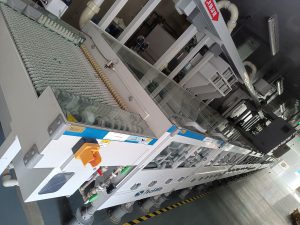
Equipment Used in Inner Layer Pretreatment
Various machines and tools are used to ensure effective inner layer pretreatment, including:
- Deburring Machines: Equipped with rotating brushes or abrasive belts for mechanical smoothing.
- Chemical Cleaning Tanks: Contain acid or alkaline solutions for oxidation removal.
- Microetching Systems: Automated systems for precise etching of copper surfaces.
- Hot Air Ovens or Vacuum Dryers: Used for moisture removal and oxidation prevention.
- Spray Chambers or Immersion Tanks: Used for adhesion promoter application.
- Automated Conveyors: Ensure uniform treatment of large PCB batches.
Quality Control Measures
Ensuring that the inner layer pretreatment process meets industry standards requires rigorous quality control measures, including:
- Surface Inspection:
- Optical inspection to detect oxidation, scratches, or surface defects.
- Thickness measurements to confirm uniform etching.
- Adhesion Testing:
- Cross-cut adhesion tests to check the bonding strength of photoresist.
- Tape tests to assess surface cleanliness.
- Microsection Analysis:
- Examination under a microscope to evaluate the surface profile and uniformity.
- Chemical Concentration Monitoring:
- Regular checks on microetching and cleaning solution concentrations to ensure consistency.
- Process Parameter Control:
- Continuous monitoring of temperature, etching time, and drying conditions to avoid variations in results.
Conclusion
Inner layer pretreatment is a fundamental step in PCB manufacturing that ensures a clean, smooth, and oxidation-free copper surface for the subsequent imaging and etching processes. This step is crucial for achieving high-quality, high-reliability PCBs, as any defects introduced during pretreatment can result in failures at later stages.
By employing advanced deburring, chemical cleaning, microetching, drying, and adhesion promotion techniques, manufacturers can significantly improve adhesion, reduce defects, and enhance electrical performance. Additionally, strict quality control measures must be implemented to ensure process stability and consistency.
As PCB technology continues to evolve, optimizing the inner layer pretreatment process will remain a key factor in improving manufacturing yields and meeting the growing demands for high-performance electronic products.

- long board pcb
- Flexible PCBs
- Special PCB
- Express Printed Circuit Board
- Pcb Prototype
- LED PCB
- PCB
- Printed Circuit Board
- Pcb meaning
- Pcb manufacturer
- Rigid pcb board
- Rigid Flex PCB
 Quote
Quote
 E-mail