1. Introduction to Impedance Control PCB
In the evolution of electronic systems, signal integrity has become a non-negotiable requirement, particularly with the increasing adoption of high-speed digital designs. At the heart of this transformation lies the Impedance Control PCB—a sophisticated solution engineered to maintain consistent electrical impedance across signal traces. While it may appear a niche concept to the uninitiated, the application of impedance control is crucial in ensuring reliable communication between components, especially in high-frequency domains.
An Impedance Control PCB is designed and manufactured with precise control over the impedance of its traces. This impedance typically refers to the resistance a signal encounters along its path, considering not only the trace resistance but also inductive and capacitive elements introduced by the trace’s geometry and its proximity to other conductors or planes.
What sets an Impedance Control PCB apart is its deliberate engineering. Every layer, material, and dimension in the board is orchestrated to support specific impedance values, commonly 50Ω or 100Ω, for single-ended and differential signal paths, respectively. These values are not randomly selected—they align with standardized protocols for USB, HDMI, Ethernet, PCIe, and other widely used interfaces.
As I reflect on the growing demands of modern systems, it becomes evident that the Impedance Control PCB has shifted from being a high-end solution to a baseline requirement in industries like telecommunications, aerospace, and medical electronics. The ramifications of poor impedance control can range from increased jitter and signal loss to complete communication failure. Thus, engineers today cannot afford to overlook this aspect during the PCB design phase.
From a personal perspective, I find that incorporating impedance control from the early design stage not only enhances the electrical performance of a circuit but also fosters a more collaborative dynamic between design and fabrication teams. It demands precise communication of stack-up details, material tolerances, and fabrication capabilities—ultimately encouraging a more holistic engineering process.
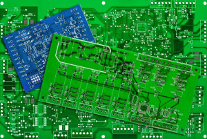
Impedance Control PCB
2. The Science Behind Impedance in Impedance Control PCB
Understanding the behavior of electrical signals within a Impedance Control PCB requires a grounding in the fundamental principles of electromagnetics and circuit theory. Impedance, at its core, is a measure of how much a conductor resists the flow of alternating current (AC), factoring in resistance (R), inductive reactance (XL), and capacitive reactance (XC). In a high-speed PCB environment, this impedance is not static; it is dynamically influenced by frequency, geometry, and dielectric materials.
Defining Characteristic Impedance in Impedance Control PCB
In the context of an Impedance Control PCB, we are typically concerned with the characteristic impedance (Z₀) of transmission lines. This is the impedance a signal “sees” as it propagates along a trace, and it is not the same as resistance in DC circuits. Instead, Z₀ is defined by the equation:
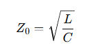
Where:
-
L is the inductance per unit length of the trace
-
C is the capacitance per unit length of the trace
Both L and C are heavily influenced by the trace width, thickness, the height of the dielectric layer beneath the trace, and the dielectric constant (Dk) of the material.
In practical terms, this means that even minor deviations in trace dimensions or material properties during manufacturing can cause significant variations in impedance, potentially degrading signal quality.
Reflections and Signal Integrity in Impedance Control PCB
One of the primary goals of an Impedance Control PCB is to prevent signal reflections. When a signal encounters a discontinuity—such as a change in impedance—it reflects back toward the source. This creates echo-like noise, which can interfere with the original signal, especially in high-speed digital systems.
Impedance mismatches lead to:
-
Signal degradation
-
Data corruption
-
Electromagnetic interference (EMI)
-
Increased crosstalk between adjacent traces
Therefore, impedance matching is not just about maintaining a number; it’s about preserving the integrity and timing of the signal throughout its journey on the PCB.
Single-Ended vs. Differential Impedance in Impedance Control PCB
In designing an Impedance Control PCB, engineers often deal with two types of impedance:
-
Single-ended impedance: This refers to a signal trace referenced to a ground plane.
-
Differential impedance: This applies to two traces carrying equal and opposite signals, such as those found in USB or Ethernet.
While single-ended traces are more common in basic designs, differential pairs are essential in high-speed applications, and maintaining the correct spacing and symmetry between these pairs is critical to controlling their impedance.
Why Impedance Control is Increasingly Critical
As devices shrink and speeds increase, the PCB has become more than a mechanical platform—it is now an essential part of the circuit. High-speed designs, operating at frequencies in the GHz range, behave less like circuits and more like transmission systems. At these speeds, the length of a trace becomes comparable to the wavelength of the signal, and impedance control becomes absolutely critical to ensure predictable signal propagation.
In my view, this shift represents a fundamental transformation in how we approach PCB design. Engineers can no longer treat layout as an afterthought. The electrical behavior of the board must be considered early and often, with impedance being one of the top concerns.
3. Types of Impedance in Impedance Control PCB
Within the domain of high-speed PCB design, impedance is not a monolithic concept. An Impedance Control PCB may encompass several distinct types of impedance, each tailored to suit specific signal routing needs. Understanding the nuances among these types is vital for optimizing performance in applications ranging from simple consumer electronics to complex aerospace systems.
1. Single-Ended Impedance in Impedance Control PCB
Single-ended impedance refers to the impedance between a signal trace and a reference plane, typically a ground or power plane. It is the most fundamental form of impedance and is commonly used in low-speed or less noise-sensitive applications.
For an Impedance Control PCB, the target single-ended impedance is often 50 ohms. This value aligns with the requirements of numerous communication standards and is relatively easy to achieve with standard FR4 dielectric material and trace geometry.
However, ensuring that this impedance remains consistent along the entire trace path is challenging. Variations in copper thickness, dielectric height, or even nearby traces can influence the actual impedance. Therefore, detailed planning and precise manufacturing are essential.
2. Differential Impedance in Impedance Control PCB
Differential impedance is a cornerstone of high-speed digital designs. It applies to a pair of traces carrying equal and opposite signals, such as those used in USB, HDMI, LVDS, PCIe, or Ethernet protocols.
In an Impedance Control PCB, differential impedance is not simply twice the single-ended impedance. Instead, it includes the effects of mutual coupling between the two traces. The spacing between these traces, their width, and the height above the reference plane collectively define the differential impedance.
Typical differential impedance targets are:
-
90 ohms for USB 2.0
-
100 ohms for Ethernet and USB 3.0
-
85 ohms for HDMI
Maintaining symmetry in differential pairs—both in geometry and length—is crucial. Any asymmetry can introduce skew, which leads to timing mismatches and signal distortion.
3. Coplanar Impedance in Impedance Control PCB
Coplanar impedance involves a signal trace surrounded by ground traces on the same layer, typically in conjunction with a ground plane beneath. This structure provides better EMI performance and allows more control over the signal path’s return current.
Coplanar configurations are more common in RF designs or when signal isolation is paramount. In an Impedance Control PCB, this method provides an extra layer of shielding and can be tuned for either single-ended or differential use, depending on the application.
While coplanar designs offer advantages, they also introduce fabrication complexity, requiring tighter control over spacing and copper clearance during etching.
4. Edge-Coupled vs. Broadside-Coupled Impedance in Impedance Control PCB
When discussing differential pairs, two coupling styles emerge: edge-coupled and broadside-coupled.
-
Edge-coupled: Both traces run on the same layer side-by-side.
-
Broadside-coupled: The traces are aligned vertically across adjacent layers.
Each method affects the differential impedance in different ways. Edge-coupling is easier to route and inspect but may be more susceptible to crosstalk. Broadside coupling provides better coupling and may offer tighter impedance control but is more difficult to implement due to layer alignment challenges.
In advanced Impedance Control PCB architectures, these coupling strategies are often chosen based on the specific electrical and mechanical constraints of the project.
5. Odd-Mode and Even-Mode Impedance in Impedance Control PCB
These less commonly discussed types are relevant in microwave engineering and precise signal simulation:
-
Odd-mode impedance refers to the impedance of one trace in a differential pair when both are active with opposite signals.
-
Even-mode impedance refers to the impedance when both carry the same signal.
While they are rarely specified in typical design briefs, understanding these parameters helps engineers model signal behavior more accurately during simulation phases of Impedance Control PCB development.
In summary, different impedance types serve different purposes, and an effective Impedance Control PCB must accommodate them based on the application’s unique requirements. Knowing which type to implement—and how to control it during both design and manufacturing—is one of the key skills separating experienced PCB engineers from the rest.
In the next section, we’ll examine how the selection of materials directly influences the ability to control impedance across the PCB.
4. Materials Selection for Impedance Control PCB
Material selection plays a foundational role in determining the electrical performance, stability, and manufacturability of an Impedance Control PCB. Even with optimal trace geometry and layer stack-up, using inappropriate materials can undermine the goal of achieving consistent and reliable impedance throughout the board.
In this section, we explore how different substrate and dielectric materials impact impedance, and what considerations engineers must make when choosing the right materials for high-frequency, high-speed applications.
Dielectric Constant (Dk) and Its Role in Impedance Control PCB
One of the most critical material parameters in an Impedance Control PCB is the dielectric constant (Dk) of the insulating material between copper layers. The Dk determines how much electric field can be stored in the dielectric medium and directly influences the capacitance per unit length of a trace.
The characteristic impedance of a trace is inversely proportional to the square root of the Dk:
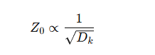
A higher Dk leads to lower impedance, while a lower Dk increases the impedance. For consistency in impedance, it is essential that the Dk is stable across frequency and temperature, which is not the case for all materials.
Standard FR4, for instance, has a Dk around 4.2 to 4.8, but it varies with frequency and manufacturing lot. High-speed applications often require more stable alternatives such as:
-
Rogers RO4000 series (Dk ≈ 3.5)
-
Isola I-Tera MT (Dk ≈ 3.0–3.4)
-
Taconic TLY or RF-35
These advanced laminates offer better control over impedance, especially when signal frequencies exceed 1 GHz.
Loss Tangent (Df) in Impedance Control PCB Materials
The dissipation factor (Df) or loss tangent measures how much signal is lost as heat during transmission. While Df doesn’t directly alter impedance, it plays a vital role in preserving signal integrity—especially in long traces and high-frequency designs.
In an Impedance Control PCB, materials with low Df are preferred to minimize signal attenuation, which indirectly helps maintain the integrity of the controlled impedance.
For example:
-
FR4 Df ≈ 0.020 (high loss)
-
Rogers RO4350B Df ≈ 0.0037 (low loss)
The lower the Df, the better the material performs at high frequencies.
Copper Foil Type and Its Impact on Impedance Control PCB
The type of copper foil used also impacts impedance control. There are mainly two types:
-
Rolled Annealed (RA) copper: Smoother surface, better for high-frequency signals.
-
Electrodeposited (ED) copper: More common and cost-effective, but rougher.
The surface roughness affects signal propagation by increasing effective resistance, which can skew impedance values slightly. For high-speed Impedance Control PCB designs, RA copper or low-profile ED copper is often recommended to reduce this variation.
Prepregs and Cores: The Building Blocks of Impedance Control PCB
Prepregs (resin-impregnated fiberglass sheets) and core materials are the primary layers between copper traces. The selection of these layers determines the dielectric thickness—a critical parameter for impedance control.
In a multilayer Impedance Control PCB, careful balancing of prepreg thickness is needed to ensure each trace maintains its intended impedance value. Modern PCB manufacturers offer detailed stack-up planning with certified Dk values for each layer to assist in this tuning process.
Material Stability and Environmental Considerations
Material performance can change under environmental stresses—such as humidity, temperature, and mechanical vibration. For mission-critical industries like aerospace or automotive, material stability is paramount.
For such applications, high-reliability materials like polyimide, PTFE, or high-Tg FR4 variants are chosen for their superior thermal and electrical stability, contributing to long-term impedance consistency.
My Reflections on Material Selection in Impedance Control PCB
From my personal engineering experience, I’ve learned that the cheapest material option often becomes the most expensive decision later in the product lifecycle. Signal issues, EMI failures, and inconsistent impedance measurements frequently trace back to underestimated material selection.
Choosing the right dielectric isn’t just about datasheets—it’s about understanding how that material performs during lamination, how it reacts to copper etching, and whether it maintains consistent properties across production batches.
I strongly believe that more collaboration between designers and fabricators in the material selection phase can drastically improve yield, reliability, and performance of Impedance Control PCB systems.
5. Trace Geometry and Its Role in Impedance Control PCB
In the design of an Impedance Control PCB, the geometry of the copper traces is one of the most influential factors in determining the characteristic impedance of signal paths. Even with the right materials and stack-up configuration, if the trace geometry is poorly defined or inconsistently manufactured, impedance control will fail. The key geometrical parameters—trace width, trace thickness, spacing, and length—must be precisely calculated and maintained throughout both the design and fabrication processes.
This section explores how each geometric element contributes to impedance behavior, the mathematical models used, and the design practices that ensure consistent and reliable performance in high-speed PCB applications.
1. Trace Width in Impedance Control PCB
Trace width is arguably the most immediately visible factor influencing impedance. For a given dielectric height and material, wider traces have lower impedance, while narrower traces have higher impedance. In Impedance Control PCB designs, the trace width must be precisely calculated to match the target impedance—usually 50 ohms for single-ended traces or 100 ohms for differential pairs.
However, it’s not just the nominal width on the Gerber file that matters. During etching, copper traces can become slightly narrower than designed due to undercutting. To account for this, designers must compensate trace widths accordingly, sometimes adjusting by several mils based on the fabricator’s capability.
Typical trace width considerations:
-
For 50Ω impedance on FR4 (Dk ~4.2), a trace width of ~10 mils with a 5 mil dielectric height is typical.
-
Differential pair spacing and symmetry also depend on trace width accuracy.
2. Trace Thickness in Impedance Control PCB
Trace thickness, often determined by the weight of copper used (e.g., 0.5 oz, 1 oz, or 2 oz), affects both resistance and impedance. Thicker copper increases capacitance and lowers impedance, which can be useful or problematic depending on the design target.
In most Impedance Control PCB configurations:
-
Inner layers usually use thinner copper for better uniformity.
-
Outer layers often start with thinner copper and are plated during the fabrication process.
For high-current applications where thick traces are necessary, designers must widen traces to compensate for the impedance reduction caused by increased thickness.
3. Trace Spacing in Differential Impedance Control PCB
In differential pairs—where two traces carry complementary signals—the spacing between the traces becomes a crucial parameter. If the traces are too close, mutual inductance and capacitance increase, resulting in lower differential impedance. Conversely, if spaced too far apart, coupling weakens, and impedance rises.
To maintain a 100Ω differential impedance, the spacing must be:
-
Tight enough for strong coupling.
-
Evenly maintained to prevent skew and reflection.
-
Adjusted based on dielectric thickness and trace width.
Example: For 100Ω differential impedance on an FR4 stack-up with 8 mil traces, spacing might need to be 6–10 mils, depending on dielectric height and Dk.
4. Trace Length and Its Role in Signal Timing
While trace length doesn’t directly affect impedance value, it significantly impacts signal timing and skew in differential pairs. In high-speed buses or serial links, even a small mismatch in length between paired traces can lead to phase errors, bit errors, and intersymbol interference.
In a well-optimized Impedance Control PCB:
-
Length matching of differential pairs is critical (within ~5 mils or less in many cases).
-
Length compensation (serpentine routing) is often used to equalize delay paths.
Moreover, sharp corners in traces can also introduce local impedance discontinuities. Best practices suggest using 45-degree bends or arcs to minimize signal reflections.
5. Controlled Etching and Manufacturing Tolerances
Designing for ideal geometry is only part of the challenge. During fabrication, trace dimensions can vary due to:
-
Etching undercut
-
Lamination pressure
-
Copper plating variability
-
Dielectric expansion or shrinkage
That’s why most professional Impedance Control PCB manufacturers provide impedance modeling services based on real-world tolerances. They simulate the actual impedance outcome using adjusted geometries to ensure that the manufactured board will meet specifications.
My Thoughts on Geometry Control in Impedance Control PCB
Through numerous projects, I’ve come to view geometry control as both an art and a science. While simulations and calculators give you a starting point, it’s only by collaborating with the fabricator—and validating through test coupons or TDR (Time-Domain Reflectometry)—that true impedance control can be achieved.
One overlooked aspect is documentation. I’ve seen impedance designs fail because critical trace geometries weren’t clearly annotated in the fabrication drawings or weren’t cross-referenced with the stack-up. Detailed drawings, complete with width/spacing callouts and layer assignment, reduce ambiguity and improve results.
Geometry in an Impedance Control PCB is not something that can be “eyeballed” or generalized—it must be quantified, verified, and communicated with precision.
6. Fabrication Process of Impedance Control PCB
Designing an Impedance Control PCB with perfect simulation models and calculated geometry is only half the story. The transition from digital layout to physical product—fabrication—is a critical phase where even minor deviations can drastically alter impedance characteristics. Maintaining tight control over materials, etching, layer alignment, and lamination is essential to ensure that the final PCB delivers the intended electrical performance.
In this section, we walk through the major steps in the PCB fabrication process, highlighting the key aspects where impedance control must be enforced, measured, and verified.
1. Stack-Up Realization and Material Preparation
The fabrication of an Impedance Control PCB begins with a stack-up defined jointly by the designer and the PCB manufacturer. Material selection, copper weights, and dielectric thicknesses must reflect what was modeled during simulation.
Key tasks:
-
Selecting specific prepreg and core combinations
-
Controlling dielectric thickness between signal layers and reference planes
-
Ensuring Dk and Df values match the simulation inputs
Most reputable fabricators use material libraries (e.g., from Isola, Rogers, or Shengyi) that are pre-characterized for impedance modeling, ensuring consistency.
2. Imaging and Etching: Defining the Traces
Impedance is highly sensitive to trace width, spacing, and copper thickness. Therefore, photolithography and etching must be carefully managed.
Etching Considerations in Impedance Control PCB:
-
Undercut: Etching can narrow trace widths, increasing impedance. Compensation is done during layout or imaging.
-
Trace tapering: Must be minimized for consistent impedance over length.
-
Copper thickness tolerance: Ensures uniform conductivity and predictable Z₀.
To mitigate risks, manufacturers often apply design-for-manufacturing (DFM) analysis to adjust trace geometries slightly before production.
3. Lamination of Multilayer Structures
Multilayer Impedance Control PCB designs require sequential lamination of prepregs and cores. The thickness between signal traces and ground planes is defined during this step.
Control points:
-
Laminate flow: If excessive, it may thin the dielectric layer, decreasing impedance.
-
Glass weave effect: Uneven resin distribution can cause impedance variation.
-
Alignment accuracy: Misalignment can cause traces to shift relative to reference planes, altering coupling and impedance.
Advanced shops use laser alignment and press cycle optimization to maintain consistency layer-to-layer.
4. Plating and Copper Management
External layers typically undergo electroplating to build up copper thickness, which directly affects trace impedance.
-
Increased thickness = Lower impedance (and lower resistance)
-
Overplating must be managed to avoid exceeding impedance margins
Fabricators often calibrate the plating process to ensure that final trace dimensions conform closely to simulated targets.
5. Via Drilling and Surface Finish
In high-frequency Impedance Control PCB designs, vias can introduce impedance discontinuities if not carefully managed.
-
Backdrilling may be used to remove unused via stubs.
-
Via-in-pad techniques offer shorter signal paths and reduced inductance.
-
Surface finishes (e.g., ENIG, immersion silver) must have uniform thickness, as inconsistencies can affect trace height.
Though vias are a small portion of the signal path, their impedance impact becomes significant at high frequencies (>1 GHz).
6. Final Inspection and Impedance Validation
Perhaps the most critical step in Impedance Control PCB fabrication is impedance measurement and verification. This is typically done using:
-
Time Domain Reflectometry (TDR): Measures impedance by sending a signal pulse and analyzing reflections.
-
Test coupons: Small, representative sections of the board fabricated alongside the main PCB for direct impedance testing.
-
Vector Network Analyzers (VNAs): Used for more complex RF/microwave boards.
Impedance tolerance is often specified as ±10% or tighter. If measured values fall outside this window, the batch may be rejected.
7. Fabricator Communication and Documentation
A successful Impedance Control PCB requires seamless communication between the designer and fabricator. This includes:
-
Stack-up drawings with dielectric thickness and copper weights
-
Impedance target values for each trace or differential pair
-
Tolerance range (e.g., 100Ω ±10%)
-
Notes on critical geometries and trace naming
Inadequate documentation is one of the most common causes of impedance failure in otherwise sound designs.
My Reflections on the Fabrication Process for Impedance Control PCB
In my experience, the gap between design intent and manufacturing reality is where many impedance issues arise. Engineers sometimes assume that once a simulation is complete, the job is done. But in reality, it’s just beginning.
I’ve learned that building a close relationship with the PCB manufacturer, understanding their process capabilities, and involving them early during the stack-up planning can avoid countless headaches. Some of the best-performing Impedance Control PCBs I’ve worked on came from open collaboration—sharing simulation data, tolerances, and discussing plating capabilities and etch-back profiles.
Impedance control isn’t achieved through layout alone—it’s realized on the shop floor, through repeatable, validated fabrication processes.
7. Tolerance and Measurement in Impedance Control PCB Manufacturing
Impedance control is not merely about achieving a fixed number; it’s about consistently maintaining impedance within an acceptable tolerance range across all boards produced. Even the most precisely designed and carefully fabricated Impedance Control PCB may still fail if actual impedance deviates beyond specification limits. This makes measurement, tolerance control, and validation essential components of high-performance PCB production.
In this section, we will explore how impedance tolerances are managed in practice, the techniques used to measure and verify impedance, and strategies to handle non-conformances when they arise.
Understanding Impedance Tolerance in Impedance Control PCB
In most high-speed electronic applications, the target impedance values are:
-
50Ω ±10% for single-ended traces
-
100Ω ±10% for differential pairs
This means that actual measured impedance should lie within:
-
45Ω to 55Ω for single-ended
-
90Ω to 110Ω for differential
In more critical applications such as DDR4 memory, PCIe Gen4, or high-frequency RF, tighter tolerances (e.g., ±5%) may be required.
Why is this important?
Signal integrity degrades significantly when reflections occur due to impedance mismatches. Even a 5Ω deviation can result in:
-
Eye diagram closure
-
Bit error rate (BER) increases
-
EMI issues
-
Loss of signal margin
Factors That Affect Impedance Tolerances
Even with a well-controlled design and stack-up, several real-world factors can push impedance out of range:
-
Dielectric thickness variation during lamination
-
Trace width fluctuation due to etch process
-
Copper plating inconsistency
-
Glass weave effects causing uneven dielectric distribution
-
Surface roughness altering effective impedance
These must be accounted for in both design and manufacturing stages of an Impedance Control PCB.
Methods for Measuring Impedance in Impedance Control PCB
1. Time Domain Reflectometry (TDR)
TDR is the most commonly used tool for measuring PCB impedance. It sends a fast rise-time pulse down the trace and detects reflected signals.
Benefits:
-
Measures impedance along the trace length
-
Identifies locations of impedance discontinuities
-
Quick and highly accurate
TDR is typically applied to test coupons—dedicated impedance structures manufactured alongside the main PCB panel. These coupons replicate the exact stack-up and trace geometry of the critical signal paths.
2. Vector Network Analyzer (VNA)
VNAs are more complex and offer detailed frequency-domain analysis, including S-parameters. They are used in RF and microwave Impedance Control PCB applications where wideband performance and phase behavior are crucial.
Advantages:
-
Frequency-specific impedance data
-
Greater insight into high-frequency performance
-
Can be used for modeling and de-embedding techniques
3. Embedded Test Structures
Some advanced PCBs incorporate embedded test traces that can be probed directly on the board. This is useful for:
-
Inline quality checks
-
Real-time process feedback
-
Volume production environments
Handling Out-of-Tolerance Impedance Results
When test results fall outside the specified tolerance, the response depends on the magnitude and cause of the deviation.
Common responses:
-
Re-evaluate etching and plating process control
-
Recalculate and adjust trace widths in design
-
Discuss stack-up and material tolerances with the vendor
-
Use statistical process control (SPC) to monitor variation over time
If the issue is caught post-fabrication, rework is typically not possible, and boards may need to be scrapped or downgraded for use in less critical applications.
Impedance Verification Protocols in Professional Settings
In a robust Impedance Control PCB process, the following verification steps are recommended:
-
Pre-fabrication modeling using software like Polar Si9000 or Ansys HFSS.
-
Fabrication of impedance coupons per impedance zone (e.g., USB, HDMI, DDR).
-
Measurement using TDR or VNA after fabrication.
-
Data logging and certification, especially for aerospace or medical applications.
-
Customer acceptance criteria clearly defined in the fabrication drawing (e.g., “Z₀ = 100Ω ±10%, TDR test, IPC-TM-650 compliance”).
My Reflections on Tolerance and Measurement in Impedance Control PCB
From my own projects, I’ve learned that tolerances must be specified early, not just in simulations but in the fabrication documents and procurement specs. In one instance, a board built with perfect design logic failed system testing. Post-mortem revealed that the impedance on certain USB 3.0 lines was off by 8 ohms—just outside the ±10% window. It turned out the supplier had substituted a slightly thicker prepreg without communicating the change.
Since then, I always emphasize two things:
-
First, tight integration between design and supply chain
-
Second, never skip TDR testing on production batches, especially for critical signal paths
You can’t control what you don’t measure. That’s the lesson.
8. Common Problems and Debugging in Impedance Control PCB
Despite careful design and fabrication, engineers often encounter challenges when working with Impedance Control PCB. These issues can manifest as signal integrity problems, unexpected impedance variations, or electromagnetic interference (EMI). Understanding common pitfalls and effective debugging techniques is essential for rapid resolution and improving future designs.
This section reviews frequent problems faced in impedance control and practical strategies to diagnose and fix them.
1. Impedance Mismatch Due to Manufacturing Variations
Problem:
Even small deviations in trace width, dielectric thickness, or copper thickness during fabrication can cause impedance to drift outside target tolerances.
Symptoms:
-
Increased signal reflections seen in TDR or eye diagrams
-
Intermittent data errors on high-speed interfaces
-
EMI emissions beyond regulatory limits
Debugging Tips:
-
Review fabrication stack-up against design documentation
-
Request impedance test coupon results from the fabricator
-
Check for known process variation in etching or plating steps
-
Collaborate with fab to tighten process controls or adjust design parameters
2. Discontinuities Caused by Via Transitions
Problem:
Vias, especially those not optimized for high-speed signals, introduce impedance discontinuities, causing signal reflections and loss.
Symptoms:
-
Signal degradation or timing issues in differential pairs
-
Unexpected impedance spikes in TDR measurements
-
Crosstalk or noise coupling near via regions
Debugging Tips:
-
Use backdrilling to remove unused via stubs and reduce reflections
-
Prefer via-in-pad or blind/buried vias for critical signals
-
Add ground stitching vias nearby to maintain return current paths
-
Simulate via structures using 3D EM tools (e.g., HFSS, SIwave)
3. Inconsistent Ground and Power Planes
Problem:
Splits or gaps in reference planes cause return path discontinuities, leading to impedance variation and EMI issues.
Symptoms:
-
Fluctuating impedance readings on controlled impedance nets
-
Unexpected noise or ground bounce on sensitive signals
-
Failures in EMI compliance testing
Debugging Tips:
-
Verify plane continuity using X-ray or plane impedance test tools
-
Avoid routing impedance-controlled traces over plane splits
-
Use multiple stitching vias to bridge plane sections
-
Design stack-ups with solid, unbroken reference layers under signal layers
4. Incorrect or Missing Documentation
Problem:
Fabricators misinterpret impedance requirements due to vague or incomplete stack-up and impedance specifications.
Symptoms:
-
Fabrication based on default or generic stack-ups
-
Unexpected impedance values outside design goals
-
Increased rework or scrap rates
Debugging Tips:
-
Provide clear stack-up drawings with all dimensions and materials
-
Specify target impedance values and tolerances in the fabrication notes
-
Include test coupon designs and acceptance criteria
-
Maintain open communication with the fabricator throughout the process
5. Signal Integrity Issues Due to Trace Geometry
Problem:
Abrupt trace bends, inconsistent spacing, or unbalanced differential pairs cause impedance disruptions and signal skew.
Symptoms:
-
Closed eye diagrams on high-speed signals
-
Timing mismatches causing data errors
-
Increased crosstalk noise between adjacent lines
Debugging Tips:
-
Replace 90° bends with 45° or curved traces
-
Ensure consistent spacing and length matching in differential pairs
-
Minimize stub traces and via transitions in critical nets
-
Use layout verification tools to check for geometry violations
6. Environmental Effects and Material Aging
Problem:
Humidity, temperature cycling, and material degradation can alter dielectric properties over time, affecting impedance stability.
Symptoms:
-
Gradual shift in impedance measurements during product lifetime
-
Intermittent failures under environmental stress testing
-
Reduced reliability in harsh operating conditions
Debugging Tips:
-
Select high-Tg, low-Df materials for critical impedance layers
-
Use conformal coatings or protective enclosures to reduce moisture ingress
-
Perform accelerated aging and environmental testing early in the design phase
-
Monitor impedance stability through periodic in-field testing if feasible
7. Testing and Measurement Errors
Problem:
Inaccurate impedance measurements due to improper test setup or equipment calibration can lead to false conclusions.
Symptoms:
-
Discrepant impedance values across different measurement sessions
-
Conflicting data between TDR and VNA instruments
-
Unexplained variation in test coupon results
Debugging Tips:
-
Calibrate measurement instruments regularly
-
Use standardized test fixtures and controlled environments
-
Train technicians on proper probing techniques
-
Cross-validate results with multiple measurement methods
My Reflections on Debugging Impedance Control PCB
From hands-on experience, many impedance-related failures stem from process and communication gaps rather than purely electrical design errors. Often, problems surface late during system integration, making diagnosis time-consuming and costly.
I’ve found that adopting a methodical debugging approach—starting from documentation review, moving through fabrication validation, and ending with detailed signal integrity analysis—helps isolate root causes efficiently.
Early and continuous collaboration with fabrication and test teams is crucial. The more information and transparency shared, the faster problems are resolved, and the more reliable the next generation of Impedance Control PCB designs become.
Conclusion: Comprehensive Insights into Impedance Control PCB
Throughout this extensive exploration of Impedance Control PCB, we have traversed the full spectrum from fundamental principles to cutting-edge future trends, highlighting the critical role of impedance management in ensuring signal integrity and reliable high-speed electronic performance.
Key Takeaways
-
Understanding impedance and its relationship with PCB materials, trace geometry, and stack-up configurations is foundational for controlled signal transmission.
-
Trace geometry—width, thickness, spacing, and length—must be meticulously designed and maintained within tight tolerances to achieve target impedance.
-
Simulation tools such as Polar Si9000, Ansys HFSS, and Keysight ADS empower engineers to predict and optimize impedance well before fabrication.
-
Fabrication processes including stack-up realization, etching, lamination, and plating must be tightly controlled to preserve impedance targets.
-
Measurement and tolerance management, especially through TDR and VNA testing of coupons, verify compliance and uncover deviations early.
-
Design best practices—from early specification to collaboration with fabricators and rigorous documentation—are essential for successful impedance control.
-
Common problems often stem from manufacturing variations, via discontinuities, grounding issues, or documentation gaps and require methodical debugging.
-
Looking forward, advanced materials, AI-enhanced simulation, additive manufacturing, embedded passives, and real-time monitoring are transforming impedance control capabilities.
My Final Thoughts
Impedance control in PCB design is a multi-disciplinary challenge that bridges electrical engineering, material science, and manufacturing expertise. Achieving consistent, reliable impedance performance demands not only deep theoretical understanding but also close collaboration across design, fabrication, and testing teams.
The journey from schematic to finished board is complex, but with rigorous attention to detail, robust processes, and embracing emerging technologies, engineers can master impedance control and deliver high-performance PCBs that meet the demands of modern electronics.

- Flexible PCBs
- Special PCB
- Express Printed Circuit Board
- Pcb Prototype
- LED PCB
- PCB
- Printed Circuit Board
- Pcb meaning
- Pcb manufacturer
- Rigid pcb board
- Rigid Flex PCB
- PCB Board
 Quote
Quote
 E-mail