Printed Circuit Board (PCB) testing is an essential process that ensures the final product functions reliably and as intended. Whether you’re a PCB manufacturer, OEM, or electronics engineer, knowing how to test a PCB board step-by-step can save you from costly rework, reduce failures in the field, and enhance your quality control. This comprehensive guide will walk you through each step in the PCB testing process, from visual inspection to advanced functional testing. We’ll also explore tools, techniques, and best practices that make testing more accurate, efficient, and scalable.
How to Test a PCB Board
1. What Is PCB Testing and Why Is It Important?
Testing a PCB board is the process of verifying its electrical performance, structural integrity, and functional operation. This includes everything from a simple continuity check to full-blown functional testing under simulated real-world conditions.
But here’s the kicker — skipping or rushing through testing can result in catastrophic failures down the line. Faulty PCBs can cause devices to overheat, malfunction, or stop working entirely. For businesses, this means warranty claims, product recalls, and damaged reputations.
PCB testing is important for a variety of reasons:
-
It validates the circuit design and layout.
-
It detects manufacturing defects such as shorts, opens, and component misplacement.
-
It ensures compliance with design specifications and quality standards like IPC-A-600 and IPC-9252.
Table: Key Benefits of PCB Testing
| Benefit | Why It Matters |
|---|---|
| Detects Faults Early | Reduces cost of rework and scrap |
| Ensures Functional Reliability | Increases customer satisfaction |
| Verifies Manufacturing Quality | Confirms that PCBs meet spec before shipment |
| Prevents Product Failures | Avoids warranty issues and field returns |
2. What Are the Different Methods for Testing a PCB?
There are multiple methods to test a PCB, and each serves a specific purpose depending on the stage of production and the complexity of the design.
Ready for the good part? No single test fits all. Effective PCB testing often involves a combination of the following techniques:
-
Visual Inspection: Used in early-stage testing to catch obvious defects.
-
Automated Optical Inspection (AOI): Uses cameras to scan the PCB for surface defects.
-
In-Circuit Testing (ICT): Measures individual component functionality while the board is unpowered.
-
Flying Probe Testing: Similar to ICT, but uses moving probes instead of a fixed fixture.
-
Functional Testing: Validates the complete system under simulated working conditions.
Table: Common PCB Testing Methods
| Method | Purpose | Best For |
|---|---|---|
| Visual Inspection | Spotting visible defects | Early-stage/manual reviews |
| AOI | Automated surface-level fault detection | Medium to high-volume production |
| ICT | Component-level electrical testing | Mass production with fixed designs |
| Flying Probe | Electrical test without test fixture | Prototypes, small batch runs |
| Functional Testing | Final performance validation | High-reliability applications |
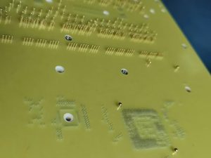
3. How Does a Visual Inspection Help in PCB Testing?
Visual inspection is the first line of defense in identifying issues in PCB fabrication or assembly. It involves checking the board for visible defects like solder bridges, missing components, or misalignments.
This is where it gets interesting — even in the age of automation, human inspection still plays a role in quality control, especially in low-volume or prototype runs.
Technicians use tools such as magnifying lamps, microscopes, and high-resolution cameras to enhance visibility. While this method isn’t foolproof, it’s quick, inexpensive, and can catch major issues early.
Visual inspection checks for:
-
Misaligned or missing components
-
Solder bridges or insufficient solder
-
Damaged traces or burnt components
-
Silkscreen errors or polarity markings
Table: Visual Inspection Checklist
| Item Checked | Defect Type | Impact if Ignored |
|---|---|---|
| Component Placement | Misalignment, missing parts | Functional failure |
| Soldering Quality | Cold joints, bridges | Intermittent connectivity |
| PCB Surface | Cracks, discoloration | Potential short circuits |
| Markings | Wrong polarity or silkscreen | Assembly or testing error |
4. What Is an AOI Test and How Does It Work?
Automated Optical Inspection (AOI) is a non-contact method that uses high-resolution cameras to inspect PCBs. It captures images and compares them with a preloaded “golden board” reference to detect abnormalities.
But here’s the kicker — AOI can check thousands of components in minutes, making it indispensable in high-volume manufacturing. It detects defects such as:
-
Component shifts or rotations
-
Missing or extra components
-
Solder joint issues
-
Tombstoning in passive components
AOI is especially effective in identifying surface-level defects that may not be picked up in electrical testing. It is often used both after solder paste application and after final component placement.
Table: AOI Detection Capabilities
| Defect Type | Detected by AOI? | Notes |
|---|---|---|
| Solder Bridges | Yes | High resolution reveals fine bridges |
| Misplaced Components | Yes | Checks X, Y, and rotation errors |
| Cold Solder Joints | Partially | Visual indicators may be subtle |
| Internal Electrical Faults | No | Requires electrical testing methods |
5. What Is In-Circuit Testing (ICT) and What Does It Cover?
In-Circuit Testing (ICT) is a powerful electrical testing method where probes contact designated test points on the board to measure component values and trace connections.
Ready for the good part? ICT can check hundreds of components in seconds. It’s especially valuable for mass production because it uses a test fixture (bed-of-nails) to rapidly connect to all test points simultaneously.
ICT typically verifies:
-
Resistors, capacitors, and inductors
-
Diodes and transistors
-
Continuity and isolation between nets
-
Presence and orientation of ICs
While ICT setup is costly and time-consuming, it pays off when testing large production volumes.
Table: ICT Test Coverage
| Component Type | Test Performed | Measured Value |
|---|---|---|
| Resistor | Resistance check | Ohms |
| Capacitor | Capacitance check | Farads |
| Diode | Forward/reverse voltage drop | Voltage (Vf) |
| Transistor | Junction tests | HFE, leakage current |
| IC Presence | Pin voltage levels | Logic High/Low |
6. How Is Flying Probe Testing Used in PCB Quality Control?
Flying Probe Testing (FPT) is a needle-based test method where probes physically move over the board to contact pads and vias. Unlike ICT, FPT doesn’t require a dedicated fixture, making it ideal for prototypes and small batches.
What’s the real story? FPT offers the flexibility to test complex or frequently changing designs without the need for expensive tooling. It also allows easy modification of test programs for new product iterations.
Flying probe systems can test:
-
Continuity and insulation resistance
-
Diodes, transistors, and capacitors
-
Polarity and orientation of components
-
Net-to-net leakage and shorts
Table: Flying Probe vs ICT Comparison
| Feature | Flying Probe | ICT |
|---|---|---|
| Test Fixture Required | No | Yes |
| Setup Time | Short | Long (fixture needed) |
| Best For | Prototypes, small runs | High-volume production |
| Test Coverage | Medium to High | Very High |
7. How to Test a PCB Board, What Is Functional Testing and Why Is It Crucial?
Functional Testing (FCT) simulates the board’s real-world operation by powering it up and verifying that it behaves as expected under normal conditions.
This is where it gets interesting — FCT is the last line of defense before a PCB is shipped or integrated into a system. It checks the board as a whole and ensures that subsystems communicate, sensors trigger, and LEDs blink when they’re supposed to.
Functional testing validates:
-
Voltage levels and power rails
-
Communication protocols (UART, SPI, I2C)
-
User interface elements (switches, displays)
-
Real-time performance under load
Table: Functional Testing Elements
| Test Parameter | Measurement Tool | What It Verifies |
|---|---|---|
| Output Voltage | Multimeter or scope | Correct voltage levels |
| Signal Timing | Oscilloscope | Pulse width, frequency |
| Sensor Response | Test environment or jig | Real-world interaction |
| Communication Bus | Protocol analyzer | Serial data integrity |
8. How Do You Perform Continuity and Short Circuit Testing?
Continuity and short circuit tests are the foundation of any PCB evaluation process. They check for open circuits (disconnected paths) and short circuits (unintended connections between two or more points).
But here’s the kicker — even a tiny short circuit can cause component failure, smoke, or even fire. Early detection is critical to avoiding damage during power-up.
These tests are often performed using a digital multimeter (DMM) in continuity mode. The technician probes between various nets to verify that:
-
Traces are connected where they should be (continuity)
-
There is no unintended connection between separate nets (short detection)
-
Ground and power planes are isolated unless intentionally bridged
For higher volume applications, automated continuity testers and test scripts are used to scan the board with predefined netlists.
Table: Continuity and Short Test Scenarios
| Test Type | Pass Condition | Fail Condition | Tool Used |
|---|---|---|---|
| Continuity Test | Resistance < 1Ω | Resistance = ∞ | Multimeter, probe |
| Short Circuit Test | Resistance = ∞ | Resistance ≈ 0Ω | Multimeter, AOI, ICT |
| Net Isolation | Nets show no electrical contact | Unintended bridging | Flying Probe, ICT |
9. How Is Solder Joint Quality Verified?
Solder joints are the mechanical and electrical connection between PCB pads and component leads. A weak or faulty solder joint is one of the most common causes of intermittent failures in electronics.
Ready for the good part? Solder joint quality can be verified using both visual and non-destructive methods. Visual inspection and AOI can catch many surface issues, but hidden joints — such as those under BGAs — require X-ray inspection.
Common defects include:
-
Cold joints: dull, grainy surfaces
-
Bridging: unintended solder connecting two pins
-
Voiding: trapped air or flux in the joint
-
Tombstoning: one lead of a chip component lifts off the pad
These defects not only affect the performance but can also reduce product lifespan significantly.
Table: Solder Joint Defects and Detection
| Defect | Symptoms | Detection Method | Impact |
|---|---|---|---|
| Cold Joint | Weak connection, no signal | AOI, visual inspection | Intermittent failure |
| Solder Bridge | Shorts, excessive current | AOI, multimeter, ICT | Burnt components |
| Voids | Air gaps reduce conductivity | X-ray inspection | Overheating, failure |
| Tombstoning | One lead not soldered | AOI, visual | No electrical contact |
10. What Software Tools Are Used in PCB Testing?
Software plays a pivotal role in both designing for testability (DFT) and executing the test routines. From layout verification to real-time signal integrity analysis, PCB testing software provides the intelligence behind efficient QA.
What’s the real story? Without smart software, even the most expensive test equipment is just metal and plastic. Today’s tools integrate with design files, automate netlist comparisons, and simulate real-world electrical behaviors before physical testing even begins.
Commonly used software tools:
-
Design Rule Checkers (DRC): Identify layout issues pre-fabrication
-
Netlist Verification Tools: Compare schematic vs. PCB traces
-
Simulation Software (e.g., SPICE): Validate analog behavior
-
Test Automation Platforms: Run ICT, FCT, and flying probe tests with scripts
Table: PCB Testing Software Functions
| Tool Type | Primary Use | Popular Tools |
|---|---|---|
| Design Verification | Rule checks, netlist analysis | Altium Designer, KiCad, OrCAD |
| Simulation | Electrical behavior modeling | LTspice, PSpice, HyperLynx |
| Automated Testing | Executing test plans, logging data | LabVIEW, TestStand, CheckSum ICT |
| Data Analysis | Visualize results, generate reports | Excel, custom dashboards, Python |
11. What Are the Common Defects Found During PCB Testing?
Even with precise manufacturing, defects are inevitable — especially in complex, multilayer or high-density PCBs. The key is knowing what to look for and having the right methods to catch them.
This is where it gets interesting — not all defects are immediately visible. Some only show up under electrical stress or thermal cycling. Others may only appear when integrated into a system.
Common PCB defects include:
-
Shorts and opens in copper traces
-
Missing, misaligned, or wrong-value components
-
Poor solder joints or bridging
-
Warped or delaminated substrates
-
ESD (Electrostatic Discharge) damage
Early detection during testing minimizes downstream failures and improves overall product reliability.
Table: Top PCB Defects and Their Causes
| Defect Type | Primary Cause | Detection Method |
|---|---|---|
| Open Circuit | Broken trace or via | Continuity test, flying probe |
| Short Circuit | Solder bridge, trace overlap | AOI, ICT, multimeter |
| Component Shift/Missing | Pick-and-place error | AOI, visual inspection |
| Bad Solder Joint | Poor reflow or wave soldering | AOI, X-ray, FCT |
| PCB Warping | Improper lamination or moisture | Visual, mechanical inspection |
12. How to Test Multilayer PCBs Effectively?
Multilayer PCBs bring complexity and performance benefits — but they also complicate testing. With signals running through multiple internal layers, traditional methods may fall short.
Ready for the good part? Effective multilayer PCB testing often combines multiple techniques: AOI for surface checks, flying probe or ICT for inner-layer continuity, and time-domain reflectometry (TDR) for impedance validation.
Critical challenges include:
-
Hidden layer-to-layer connections
-
Internal shorts or opens
-
High-speed signal integrity issues
Using TDR and cross-section analysis allows testing of buried vias, backdrilled connections, and impedance-controlled traces — all essential for telecommunications, aerospace, and computing.
Table: Multilayer PCB Testing Tools
| Test Method | Detects | Best For |
|---|---|---|
| Flying Probe | Shorts, opens across layers | Low-volume complex boards |
| TDR | Impedance mismatch, delay skews | High-speed digital circuits |
| X-Ray | Internal structure, via alignment | High-layer-count PCBs |
| Microsection Analysis | Laminate integrity, drill defects | Root cause analysis |
13. What Are the Best Practices for Reliable PCB Testing?
PCB testing isn’t just about tools — it’s also about discipline. Following best practices ensures consistency, accuracy, and traceability across production batches and product generations.
But here’s the kicker — even advanced test equipment can’t compensate for poor process discipline. Establishing repeatable, documented test routines is non-negotiable in high-reliability sectors like aerospace, medical, and automotive.
Recommended best practices:
-
Always test before and after assembly
-
Maintain a detailed inspection checklist
-
Use ESD protection during testing
-
Log and analyze failure data to improve design and process
-
Integrate design-for-testability (DFT) principles early
Table: Best Practices Checklist
| Practice | Why It Matters | Consequence if Ignored |
|---|---|---|
| Test Before & After Assembly | Catches defects at each stage | Overlooking early-stage errors |
| Use DFT Design Rules | Simplifies test point access | Limited test coverage |
| Document All Test Results | Ensures traceability and compliance | Inconsistent quality control |
| Perform ESD-Safe Handling | Prevents latent component failures | Unexpected field failures |
14. How Does PCB Testing Differ for Prototype vs. Mass Production?
Testing a prototype board is very different from testing a mass-produced one. In prototyping, flexibility, speed, and manual methods are prioritized. For production, automation, speed, and cost efficiency dominate.
What’s the real story? In prototyping, test jigs are rarely used. Engineers often rely on flying probe testers, multimeters, and oscilloscopes. But for production, fixed ICT fixtures, AOI machines, and robotic FCT stations are key to scaling.
Key differences:
-
Test coverage may be deeper in prototyping to uncover unknown faults
-
Mass production often involves parallel testing for speed
-
Cost-per-unit is more critical in production environments
Table: Prototype vs. Production Testing
| Aspect | Prototype | Mass Production |
|---|---|---|
| Test Method | Manual, flexible | Automated, fixture-based |
| Cost Sensitivity | Low | High |
| Setup Time | Short | Long (fixture required) |
| Test Depth | High (exploratory) | Balanced (speed-focused) |
15. How to Choose the Right Testing Method for Your PCB Project?
Selecting the right testing method depends on several factors: board complexity, production volume, functional requirements, and budget.
This is where it gets interesting — what works for a prototype might be overkill (or underpowered) for a production run. Similarly, a high-speed RF board requires different testing than a low-frequency power supply.
Decision-making factors include:
-
Volume: Small batches = flying probe; large volumes = ICT
-
Complexity: More layers = TDR, X-ray, FCT
-
Cost: Balance fixture cost vs. test coverage
Combining multiple methods often yields the best results, especially for high-reliability or mission-critical boards.
Table: Testing Method Selection Matrix
| Criteria | Recommended Method | Example Application |
|---|---|---|
| Low Volume | Flying Probe, Manual Check | R&D, prototypes |
| High Volume | ICT, AOI, FCT | Consumer electronics |
| High Frequency | TDR, Functional Test | RF modules, routers |
| Power Boards | FCT, Thermal Testing | Power supplies, converters |
Conclusion
Testing a PCB board step-by-step is not just a technical necessity — it’s a competitive advantage. From visual inspection to functional testing, each method plays a role in delivering reliable, high-quality electronics. By understanding the purpose and strengths of each testing approach, businesses can streamline production, reduce failures, and improve customer satisfaction.
Whether you’re testing a prototype or scaling for mass production, integrating these practices into your QA process will pay dividends in performance, reputation, and bottom-line results.
FAQ
Q1: What is PCB testing?
PCB testing is the process of verifying the functionality, electrical integrity, and quality of a printed circuit board using various manual and automated methods.
Q2: How does in-circuit testing work?
In-circuit testing uses probes to contact test points and measure electrical values such as resistance, capacitance, and continuity without powering the board.
Q3: What is the difference between AOI and functional testing?
AOI checks surface defects using cameras, while functional testing powers up the board and checks real-world performance.
Q4: How do you test for short circuits on a PCB?
Short circuits are tested using a multimeter or automated tester to check for unintended low-resistance paths between isolated nets.
Q5: Why is functional testing critical for PCBs?
Functional testing ensures that the board operates as intended under actual conditions, reducing the chance of failure after deployment.

- long board pcb
- Flexible PCBs
- Special PCB
- Express Printed Circuit Board
- Pcb Prototype
- LED PCB
- PCB
- Printed Circuit Board
- Pcb meaning
- Pcb manufacturer
- Rigid pcb board
- Rigid Flex PCB
 Quote
Quote
 E-mail