In this article, we will explore everything you need to know about how to make a PCB (Printed Circuit Board), from the design process to assembly and testing. PCBs are the backbone of modern electronics, used in everything from smartphones to industrial equipment. Whether you’re a beginner or looking to refine your PCB-making skills, this guide will provide you with essential knowledge and tips for successful PCB fabrication.
PCB manufacturing can seem complex, but by breaking down the process into manageable steps, you can create high-quality, reliable PCBs. This guide will take you through every stage of the PCB fabrication process, including choosing materials, designing the layout, etching, and assembly, as well as testing for functionality. Ready for the good part? By following these steps, you can successfully make your own PCB, whether for a simple prototype or a mass-produced product.
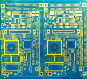
How to Make PCB
1. Introduction to PCB Making
PCB making involves creating a physical board that connects and supports various electronic components. A PCB serves as the foundation for electronic circuits, with copper traces that carry electrical signals, and pads for components such as resistors, capacitors, and chips. The primary goal of making a PCB is to design and fabricate a circuit that functions efficiently, is easy to assemble, and is reliable for long-term use.
What’s the real story? The process may seem daunting, but understanding the basic steps and materials involved can make the process more manageable and accessible. The key to a successful PCB is meticulous planning, including accurate design and choosing the right materials and processes.
The fabrication process typically involves multiple stages: creating the PCB design, transferring the design to the board, etching away excess copper, drilling holes for components, applying the solder mask, and assembling the components. These steps work together to ensure that the PCB functions as intended and can be assembled into a finished product.
Table 1: Basic PCB Manufacturing Steps
| Step | Description | Key Tools or Materials |
|---|---|---|
| Design | Create the schematic and layout design | PCB design software (e.g., Eagle) |
| Etching | Remove excess copper to form circuit traces | Etching solution (ferric chloride) |
| Drilling | Drill holes for component leads and vias | Drill machine, CNC router |
| Solder Mask Application | Apply protective layer over traces and pads | Solder mask material |
| Component Placement | Place and solder components onto the PCB | Soldering iron, solder paste |
2. Basic Components and Materials for Making PCBs
Creating a PCB requires several key materials and components. Ready for the kicker? The choice of materials affects not only the performance and durability of the PCB but also its cost and the complexity of the manufacturing process.
The most common material for the PCB base is FR4, a fiberglass-reinforced epoxy laminate. This material offers good electrical insulation, mechanical strength, and is cost-effective. For more demanding applications, polyimide may be used for flexible PCBs, and ceramic materials are employed for high-power applications. The copper foil that forms the conductive layer is typically bonded to the base material, and additional layers may be added for multi-layer PCBs.
Beyond the base materials, other critical components include solder mask (to protect the copper traces), silkscreen (for labeling components), and vias (small holes that connect different layers of the PCB). Understanding how these materials come together is essential for producing high-quality, functional PCBs.
Table 2: Common PCB Materials and Their Properties
| Material | Description | Application |
|---|---|---|
| FR4 | Fiberglass-reinforced epoxy laminate | Standard PCBs, consumer electronics |
| Polyimide | Flexible, heat-resistant material | Flexible PCBs, medical devices |
| Ceramic | High thermal conductivity material | High-power, LED applications |
| Copper | Conductive metal used for traces | Standard PCBs, high-speed circuits |
3. How to Make PCB, Designing a PCB: Software and Tools
Before starting the physical PCB fabrication process, a design must be created. This is where PCB design software plays a crucial role. Let’s dive in—designing a PCB is where the magic happens, and a good design will determine the board’s performance and ease of assembly.
Popular design software includes Eagle, KiCAD, and Altium Designer. These tools allow designers to create schematics, layout the PCB, and define the electrical connections between components. What’s the real story? Most of these software tools offer features such as component libraries, design rule checks (DRC), and simulation tools to test and verify the design before fabrication.
Designing a PCB involves creating a schematic diagram that shows how the components will be connected electrically. Once the schematic is complete, it’s translated into a layout where components are placed on the board, and electrical traces are routed. The key is to optimize space, ensure clear routing of signals, and minimize interference.
Table 3: Popular PCB Design Software and Features
| Software | Features | Best For |
|---|---|---|
| Eagle | Schematic capture, PCB layout, design rules checks | Beginners, hobbyists |
| KiCAD | Open-source, multi-layer support | Open-source enthusiasts, small businesses |
| Altium Designer | Advanced routing, 3D modeling, high-speed design | Professional, large companies |
4. The PCB Making Process: Step-by-Step Guide
The PCB fabrication process involves several stages, each with its own set of tools and techniques. But here’s the kicker? The process can vary slightly depending on the complexity of the design and the materials used. However, the general flow remains the same.
Step 1: Preparing the PCB Design File
After creating the design in PCB software, the first step is to convert the design into a format that can be used for fabrication. This is typically done by exporting the design as a Gerber file. The Gerber file contains information about the copper traces, component placement, and other essential details for the PCB manufacturing process.
Step 2: Printing the Design onto Copper Boards
Once the design is ready, it is printed onto a copper-clad board. This is done by applying a photoresist material to the board and then using UV light to transfer the design. The areas exposed to the UV light harden, while the unexposed areas are washed away.
Step 3: Etching the Copper to Create Traces
The copper board is then placed in an etching solution (usually ferric chloride), which removes the unwanted copper, leaving behind the copper traces that form the circuit pathways. This is where precision is critical—too much etching can damage the design, while too little can leave unwanted copper behind.
Step 4: Drilling Holes for Vias and Components
After etching, small holes are drilled for the vias (which allow connections between layers in multi-layer PCBs) and component leads. These holes are drilled using a high-precision drill, ensuring that the components fit correctly.
Step 5: Applying the Solder Mask
A protective layer called the solder mask is applied to the PCB. This layer helps protect the copper traces from oxidation and prevents accidental soldering of components to the wrong pads. The solder mask is typically green, but other colors are available.
Step 6: Adding the Silkscreen Layer
The final step is to apply the silkscreen layer, which is used for labeling the PCB with component values, logos, and other identifiers. The silkscreen is printed on top of the solder mask.
Table 4: PCB Manufacturing Process
| Step | Description | Tools or Materials Used |
|---|---|---|
| Design Preparation | Convert design to Gerber file | PCB design software, Gerber viewer |
| Printing the Design | Transfer the design to a copper-clad board | UV exposure unit, photoresist |
| Etching | Remove excess copper to form circuit traces | Ferric chloride, etching tank |
| Drilling | Drill holes for vias and components | CNC drill, drill press |
| Solder Mask Application | Apply protective solder mask | Solder mask material, curing oven |
| Silkscreen Printing | Add labeling to the PCB | Silkscreen ink, printing press |
5. How to Etch a PCB at Home
Etching a PCB at home is a popular DIY project for hobbyists and engineers alike. What’s the real story? While it requires some patience and attention to detail, it’s completely possible to etch your own PCBs at home with the right materials and tools.
Materials Needed
- Copper-clad PCB material
- Ferric chloride or other etching solution
- Laser printer and glossy paper
- Iron or laminator for transferring design
Step-by-Step Guide
- Prepare the Design: Print the PCB design onto glossy paper using a laser printer.
- Transfer the Design: Place the printed design on the copper board, and use an iron or laminator to transfer the toner onto the board.
- Etch the PCB: Submerge the copper board in ferric chloride to etch away the excess copper.
- Clean the Board: After etching, clean the board to remove any remaining toner and etching solution.
Table 5: DIY PCB Etching Materials and Tools
| Material/Tool | Description | Cost |
|---|---|---|
| Copper-clad PCB | Base material for PCB fabrication | Low-cost, available online |
| Ferric Chloride | Etching solution to remove copper | Inexpensive, effective |
| Glossy Paper | Paper used for transferring design | Low-cost, readily available |
| Iron or Laminator | Heat source for transferring design to copper board | Affordable, common household item |
6. Drilling and Preparing Vias
Drilling holes for vias is an essential step in the PCB manufacturing process, especially in multi-layer PCBs. Ready for the good part? The precision of this step is crucial for ensuring that the vias properly connect the layers of the PCB.
Vias are small holes drilled through the PCB that allow electrical signals to pass from one layer to another. These vias are typically plated with copper to maintain the electrical connection. There are several types of vias, including blind vias, buried vias, and through-hole vias, each serving a different purpose depending on the design of the PCB.
Table 6: Types of Vias in PCB Manufacturing
| Type of Via | Description | Application |
|---|---|---|
| Through-hole Via | A via that passes completely through the PCB | Standard multi-layer PCBs |
| Blind Via | A via that connects the outer layers to inner layers | Used in high-density designs |
| Buried Via | A via that connects only inner layers | High-density multi-layer PCBs |
7. Conclusion: Mastering the Art of PCB Making
In conclusion, making your own PCBs can be a rewarding experience, whether for prototyping or developing new products. What’s the real story? Mastering PCB fabrication allows you to have complete control over your electronic designs, offering flexibility and customization.
By understanding the basics of PCB design, etching, drilling, and assembly, you can create high-quality boards that meet your performance needs. Whether you choose to do it yourself or outsource to a professional manufacturer, knowing how PCBs are made will give you a deeper appreciation for the role they play in the electronics we use every day.gh testing. Common methods include automated optical inspection (AOI), in-circuit testing, and functional testing.
8. Adding Solder Mask and Silkscreen
Once the PCB has been etched and drilled, it’s time to apply the solder mask and silkscreen layers. Ready for the kicker? These final steps are crucial to protect the PCB and ensure that it is properly labeled for assembly and usage. The solder mask and silkscreen are what make the PCB ready for real-world use.
Solder Mask
The solder mask is a layer of material applied over the copper traces to protect them from oxidation, prevent short circuits, and ensure that only the designated pads and leads are exposed for soldering. It also helps avoid accidental soldering of components to the wrong pads. This protective layer is typically green, but it can come in other colors, such as red, blue, or black, depending on the manufacturer’s preference.
To apply the solder mask, the PCB is coated with a photo-sensitive material, which is then exposed to ultraviolet (UV) light through a mask. The areas that are exposed to UV light become hardened, and the unexposed areas are washed away, leaving behind the protective mask over the copper traces.
Silkscreen
The silkscreen layer is used to add markings such as component labels, logos, and other critical information to the surface of the PCB. These markings make it easier for technicians to assemble the PCB and ensure the correct placement of components. The silkscreen is typically printed in white, though other colors can be used. It’s printed onto the surface of the PCB after the solder mask has been applied, ensuring that it doesn’t interfere with the soldering process.
Table 7: Solder Mask and Silkscreen Processes
| Process | Description | Purpose |
|---|---|---|
| Solder Mask | Apply a protective layer to copper traces | Prevents oxidation, avoids soldering errors |
| Silkscreen Printing | Apply labels and markings for component placement | Helps with assembly and identification |
9. PCB Assembly: How to Place and Solder Components
The next step in the PCB making process is component assembly. This is where the design comes to life, as the components are placed onto the PCB and soldered into place. Ready for the good part? The assembly process can either be done by hand or through automated methods, depending on the scale of production.
Component Placement
The first step in assembly is to place the components onto the PCB. Components are typically either through-hole or surface-mount. Through-hole components have leads that pass through holes in the PCB, while surface-mount components sit on the surface of the board. Proper placement is critical to ensure the board’s functionality and avoid issues during the soldering process.
For small-scale production or prototyping, components are often placed by hand. For large-scale production, pick-and-place machines are used to automatically place the components onto the PCB, improving speed and accuracy.
Soldering
Once the components are placed, the next step is soldering. Soldering is the process of creating a permanent electrical connection between the PCB pads and component leads by melting solder. There are several methods for soldering, including:
- Wave soldering: A method used for through-hole components, where the board is passed over a wave of molten solder.
- Hand soldering: Manual soldering for prototyping or small batches.
- Reflow soldering: Used for surface-mount components, where the solder is applied to the board and then heated in an oven to create solder joints.
Proper soldering ensures reliable connections and reduces the risk of poor performance or board failure.
Table 8: Common Soldering Methods
| Method | Description | Best For |
|---|---|---|
| Wave Soldering | Molten solder is passed over the PCB to solder through-hole components | Large production, through-hole components |
| Hand Soldering | Manual soldering with a soldering iron | Prototyping, small-scale production |
| Reflow Soldering | Solder paste is applied, then heated in an oven | Surface-mount components |
10. Testing Your PCB for Functionality
After assembly, it’s crucial to test the PCB to ensure that it works as intended. Ready for the kicker? Testing is a key step that helps identify any issues in the design, assembly, or manufacturing process that could lead to failures in the final product. There are several types of tests that can be performed on PCBs.
Electrical Testing
In-circuit testing (ICT) checks the electrical connections between components on the PCB. This test ensures that there are no short circuits, open circuits, or incorrect connections between pads. During ICT, a probe is used to test each individual component on the PCB for continuity and proper functionality.
Functional Testing
Once the basic electrical connections are verified, functional testing simulates real-world conditions to ensure that the PCB performs as expected in the final application. This type of testing checks for signal integrity, response times, and power consumption, and it ensures that the board will meet performance standards.
Visual Inspection
Automated optical inspection (AOI) is commonly used for visual inspection, which identifies any surface defects like misaligned components, soldering errors, or cracks in the PCB. AOI systems can quickly scan the board and flag any irregularities for further inspection.
Table 9: Types of PCB Testing
| Testing Type | Description | Purpose |
|---|---|---|
| In-Circuit Testing | Checks electrical continuity and connectivity | Ensures proper connections |
| Functional Testing | Tests the PCB under real-world conditions | Verifies performance and functionality |
| Visual Inspection | Uses automated optical systems to inspect for defects | Detects surface-level issues like misalignment |
11. Advanced Techniques for Making High-Quality PCBs
As technology advances, high-quality PCBs are required to meet the increasing demand for compact, high-performance electronic devices. What’s the real story? The techniques used in PCB making are constantly evolving, with advancements in multi-layer PCB fabrication, HDI (High-Density Interconnect) technology, and flexible PCB designs.
Multi-Layer PCBs
Multi-layer PCBs are used to create more complex circuits that require additional layers for signal routing, power distribution, and grounding. These PCBs are used in high-performance electronics like computers, medical devices, and telecommunications equipment. Manufacturing multi-layer PCBs requires precise alignment and careful layer stacking to ensure signal integrity.
HDI PCBs
HDI PCBs use smaller vias, finer traces, and increased component density to create ultra-high-density circuits. These PCBs are used in smartphones, wearables, and other compact devices where space is limited, and performance is crucial. Manufacturing HDI PCBs requires specialized techniques like laser drilling and microvia plating.
Flexible PCBs
Flexible PCBs are made from materials like polyimide and are used in applications where the board needs to bend or flex. These are commonly used in wearable devices, medical instruments, and robotics. Flexibility introduces unique challenges in manufacturing, such as ensuring that the PCB maintains its electrical integrity despite physical movement.
Table 10: Advanced PCB Techniques
| Technique | Description | Application |
|---|---|---|
| Multi-Layer PCBs | PCBs with more than two layers | High-performance electronics, medical devices |
| HDI PCBs | Ultra-high-density designs with microvias and fine traces | Smartphones, wearables, compact electronics |
| Flexible PCBs | PCBs made from flexible materials like polyimide | Wearable devices, medical equipment |
12. The Future of PCB Making
As demand for faster, smaller, and more efficient electronics grows, the future of PCB making is filled with exciting possibilities. Ready for the good part? Emerging technologies like 3D printing, 5G communication, and wearable electronics are driving the need for more innovative PCB manufacturing techniques.
3D Printed PCBs are a game-changer for rapid prototyping, as they allow designers to create complex, custom boards quickly and affordably. This technology is being explored for low-volume manufacturing and specialized applications where traditional PCB fabrication may not be feasible.
5G technology is also pushing the need for high-speed, high-density PCBs that can support higher data transmission rates. As these networks continue to expand, PCBs will play a crucial role in supporting the infrastructure.
Table 11: Emerging PCB Manufacturing Technologies
| Technology | Description | Impact on PCB Industry |
|---|---|---|
| 3D Printed PCBs | Use of 3D printing for rapid, custom PCB creation | Speeds up prototyping and custom designs |
| 5G and High-Speed Designs | Increased need for PCBs that can handle high-speed data transmission | Drives demand for high-performance, high-density PCBs |
13. Conclusion: Mastering the Art of PCB Making
In conclusion, making PCBs is a crucial skill for anyone involved in electronics design and manufacturing. Ready for the kicker? Whether you’re creating a simple prototype or working on a mass-produced electronic device, understanding the steps involved in PCB making—design, fabrication, testing, and assembly—ensures that you can create high-quality, reliable PCBs that meet your design specifications. With advancements in PCB technology, the possibilities are endless, and mastering this process opens up a world of opportunities in the electronics industry.
FAQ Section
Q1: What is PCB fabrication?
A1: PCB fabrication is the process of creating a printed circuit board from a design file, involving steps such as etching, drilling, applying solder mask, and placing components to create functional electronic circuits.
Q2: How do you design a PCB?
A2: Designing a PCB involves creating a schematic, laying out the components on a board, and routing the electrical connections. Design software like Eagle or Altium is used to facilitate this process.
Q3: How do you etch a PCB at home?
A3: To etch a PCB at home, you can print the design onto a copper board, transfer it using heat, then etch away the excess copper using ferric chloride or a similar solution.
Q4: What is HDI PCB technology?
A4: HDI (High-Density Interconnect) PCB technology involves using fine traces and small vias to create high-density, compact circuits. These PCBs are used in devices like smartphones and wearables.
Q5: How do you ensure quality during the PCB manufacturing process?
A5: Quality is ensured through steps such as design verification, automated inspection, in-circuit testing, and compliance with industry standards.

- long board pcb
- Flexible PCBs
- Special PCB
- Express Printed Circuit Board
- Pcb Prototype
- LED PCB
- PCB
- Printed Circuit Board
- Pcb meaning
- Pcb manufacturer
- Rigid pcb board
- Rigid Flex PCB
 Quote
Quote
 E-mail