Introduction to Hot Air Solder Levelling Technology
Printed Circuit Boards (PCBs) are fundamental to modern electronics, serving as the backbone for almost all electronic devices. The quality and reliability of a PCB are directly affected by the processes involved in its manufacture, especially surface finishing. Among these, Hot Air Solder Levelling (HASL) technology has remained a widely adopted surface finish method due to its cost-effectiveness, excellent solderability, and robustness.
Surface finishing is a critical step in printed circuit board (PCB) manufacturing, ensuring the protection of copper traces from oxidation and providing a solderable surface for component assembly. Among the various surface finishing techniques, Hot Air Solder Leveling (HASL) has been a cornerstone for decades due to its cost-effectiveness and reliability. This guide delves into the technical intricacies of HASL technology, exploring its evolution, operational workflows, and role in modern electronics manufacturing. Hot Air Solder Levelling technology involves coating the exposed copper surfaces of a PCB with molten solder and then removing the excess solder using a stream of hot air. This process not only provides a protective coating against oxidation but also ensures that the solder pads are leveled, thus enabling consistent component placement and solder joint formation during assembly.
This surface finish method has evolved significantly since its inception. Early methods of HASL were limited in their ability to provide uniform coating across fine-pitch components and micro vias. However, technological advancements have allowed for more precise control, with both vertical and horizontal leveling machines available today to meet the demands of various circuit board complexities.
As PCB technologies continue to push toward finer pitches, higher densities, and lead-free requirements, HASL has had to compete with other finishing methods such as ENIG (Electroless Nickel Immersion Gold), OSP (Organic Solderability Preservative), and immersion silver or tin. Still, Hot Air Solder Levelling technology maintains its relevance in numerous applications due to its low cost, mechanical robustness, and compatibility with traditional assembly processes.
This article offers an in-depth analysis of the entire HASL process, from materials and equipment to the detailed methodology, quality control mechanisms, environmental considerations, and comparative performance with other PCB finishing techniques. Additionally, it explores the challenges, improvements, and innovations associated with Hot Air Solder Levelling technology, particularly in the context of lead-free compliance and miniaturized electronic assemblies.
Whether you are a PCB design engineer, manufacturing technician, or quality assurance professional, understanding the intricacies of HASL technology is essential for ensuring high performance and reliability in your final products. This comprehensive guide will equip you with all the necessary knowledge to appreciate and effectively implement Hot Air Solder Levelling technology within your production ecosystem.
Hot Air Solder Levelling technology
1. Overview and Evolution of Hot Air Solder Levelling Technology
1.1 Historical Context of Hot Air Solder Levelling Technology
The emergence of Hot Air Solder Levelling technology dates back to the early decades of mass electronic production, where manufacturers needed a reliable, low-cost method to preserve copper pads and improve solderability. Initially, HASL was developed as a solution for replacing the fragile and corrosion-prone bare copper finish, which would oxidize easily and hinder solder adhesion.
In early implementations, the process used eutectic tin-lead solder, and was largely manual or semi-automated. Vertical HASL machines were standard, and the process lacked precision, especially when dealing with fine-pitch or densely packed PCBs. As surface-mount technology (SMT) became widespread in the 1980s and 1990s, the HASL process evolved to meet stricter flatness and reliability requirements.
1.2 Evolution to Modern HASL Equipment
The development of horizontal HASL systems marked a significant advancement in the consistency and flatness of the solder coating. Horizontal systems offered more controlled dwell time in solder baths, precise hot air knives positioning, and uniform heating—all of which led to flatter finishes essential for high-speed SMT pick-and-place machines.
Additionally, HASL adapted to the introduction of lead-free solder alloys, aligning with RoHS (Restriction of Hazardous Substances) directives in Europe and other global markets. This transition brought new challenges, including higher solder bath temperatures, increased oxidation rates, and different wetting behaviors.
Modern Hot Air Solder Levelling technology supports a wide range of PCB sizes, layer counts, and copper thicknesses, making it suitable for both simple and moderately complex PCBs. While not ideal for ultra-fine BGA or HDI boards, it remains highly relevant in the industrial, automotive, power supply, and consumer electronics sectors.
2. Technical Details of the Hot Air Solder Levelling Process
2.1 Pre-treatment of the PCB Surface
Before a PCB enters the HASL system, it undergoes extensive cleaning and preparation. This step is critical because any organic contamination, oxide layer, or particulate matter on the copper surface will inhibit solder adherence.
The steps typically include:
-
Micro-etching: A light chemical etching process to remove surface oxides.
-
Rinsing: Removal of residual chemicals using deionized water.
-
Drying: Preheating the PCB to eliminate moisture and prepare it for immersion in molten solder.
2.2 Application of Flux
A flux coating is applied to the copper areas to promote solder wetting and remove any remaining oxides. The type of flux used in Hot Air Solder Levelling technology can vary based on the solder alloy and equipment. It must ensure thermal stability, minimal residues, and non-corrosive properties.
Flux is applied via:
-
Spray coating
-
Foam fluxing
-
Wave fluxing
After fluxing, the PCB is preheated to drive off volatiles and improve the flow of solder.
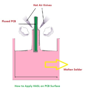
2.3 Immersion in Molten Solder
The PCB is immersed in a bath of molten solder—typically tin-lead (Sn63Pb37) or lead-free alloys like SAC305 (tin-silver-copper). The solder must be kept at precise temperature (183–260°C depending on the alloy), and the PCB must be held at a controlled immersion depth and duration.
The goal of this step is to coat all exposed copper pads with a uniform layer of solder.
2.4 Air Knife Levelling
Immediately after solder immersion, high-pressure hot air knives are used to blow off excess solder and level the remaining solder across the pads.
Important variables include:
-
Air pressure (2–6 bar)
-
Air temperature (220–280°C)
-
Angle and distance of the air knives
-
Conveyor speed
Horizontal machines provide more uniformity in this stage compared to older vertical systems.
2.5 Post-treatment and Cleaning
Once levelling is complete, the PCB is cooled and cleaned to remove flux residues. In some cases, saponification or semi-aqueous cleaning is used to deal with no-clean or water-insoluble fluxes.
Thorough cleaning is essential to:
-
Prevent long-term corrosion
-
Maintain solderability
-
Avoid reliability failures such as dendritic growth or ionic contamination
3. Equipment Used in Hot Air Solder Levelling Technology
3.1 Horizontal vs. Vertical HASL Machines
There are two main types of equipment used in Hot Air Solder Levelling technology:
-
Vertical HASL Machines: More compact, but less uniform in solder distribution. Suitable for lower-volume or simpler PCBs.
-
Horizontal HASL Machines: Larger, more advanced, and deliver superior results for SMT boards due to better flatness and repeatability.
3.2 Fluxing Units
High-precision fluxing systems enable accurate and repeatable flux deposition, including:
-
Foam fluxers for cost efficiency
-
Spray fluxers for precision and low-residue applications
3.3 Solder Baths
These units maintain solder at stable temperatures using PID-controlled heaters, inert gas blanketing, and solder agitation systems.
3.4 Air Knife Systems
Advanced air knife modules offer:
-
Variable pressure and temperature control
-
Optimized nozzle geometries
-
Closed-loop feedback for consistent levelling
4. Advantages and Limitations of Hot Air Solder Levelling Technology
4.1 Advantages
-
Excellent solderability: The exposed pads have fresh solder coating, ensuring strong joints.
-
Oxidation protection: Coated surfaces are shielded from atmospheric corrosion.
-
Cost-effective: Less expensive than ENIG, immersion tin, or silver.
-
Robust: Withstands multiple thermal cycles, ideal for wave soldering or through-hole assembly.
4.2 Limitations
-
Non-flat surface: Not ideal for ultra-fine-pitch or BGA components.
-
Thermal stress: High temperatures may damage delicate PCBs or components.
-
Environmental impact: Traditional SnPb solder is not RoHS-compliant, requiring lead-free variants with higher energy consumption.
5. Quality Control in Hot Air Solder Levelling Technology
5.1 Importance of Quality Assurance in Hot Air Solder Levelling Technology
In any PCB manufacturing process, quality control plays a critical role in ensuring the functionality, reliability, and lifespan of the final product. This importance is magnified in Hot Air Solder Levelling technology, where even minor deviations in the process can result in significant defects such as poor solderability, uneven pad coverage, or damaged substrates.
To address these challenges, manufacturers establish rigorous quality control protocols at every stage of the HASL process. From solder composition analysis to real-time monitoring of air knife pressure, every parameter is scrutinized and calibrated to meet stringent IPC standards.
5.2 Inspection After HASL Processing
After the HASL process is complete, PCBs undergo several inspection and testing steps to validate solder coverage and surface quality. These include:
-
Visual Inspection: Carried out manually or with automated optical inspection (AOI) tools, focusing on solder thickness, pad coverage, bridging, and solder balls.
-
Microsection Analysis: Cross-sectional views help assess pad adhesion, solder coverage depth, and the impact of thermal stress on internal layers.
-
Solderability Testing: Using wetting balance or dip-and-look methods, these tests determine if the solder finish allows for reliable assembly in downstream processes.
5.3 Common Defects in Hot Air Solder Levelling Technology
Despite careful control, the process may still result in the following issues:
-
Excess solder bridging: Caused by improper air knife settings.
-
Insufficient solder coating: Typically the result of low solder bath temperatures or contaminated flux.
-
Pad lifting or delamination: Often due to excessive thermal shock during immersion.
-
Solder balls: Caused by flux residue or splashing during air knife levelling.
Each defect type requires a corrective action protocol that may involve equipment recalibration, process re-engineering, or changes in consumables such as flux or solder alloy.
5.4 Calibration and Equipment Maintenance
Scheduled maintenance of Hot Air Solder Levelling technology equipment is essential for consistent results. This includes:
-
Regular cleaning of solder bath tanks to prevent dross accumulation.
-
Recalibration of PID controllers for bath temperature control.
-
Verification of air knife nozzle alignment and wear.
-
Monitoring of exhaust and filtration systems for fume control.
5.5 Certification and Compliance Standards
Most HASL-finished PCBs must meet international quality standards. These include:
-
IPC-6012: Qualification and performance specification for rigid PCBs.
-
IPC-A-600: Acceptability of printed circuit boards.
-
RoHS Compliance: If lead-free solder is used.
Conformance to these standards ensures that the product meets the reliability expectations of automotive, aerospace, industrial, and medical electronics sectors.
6. Comparative Analysis with Other Surface Finishes
6.1 Hot Air Solder Levelling Technology vs. ENIG
Electroless Nickel Immersion Gold (ENIG) is often compared to HASL for its superior flatness and suitability for fine-pitch components. Key differences include:
-
Cost: HASL is significantly cheaper than ENIG.
-
Flatness: ENIG offers better surface planarity.
-
Oxidation Resistance: ENIG provides long-term protection, especially in storage.
-
Solderability: HASL offers better immediate solderability.
6.2 Hot Air Solder Levelling Technology vs. Immersion Tin
Immersion tin is another RoHS-compliant finish offering good solderability and flatness. However:
-
Tin is susceptible to whiskering, which can create shorts.
-
The finish is less robust during multiple reflows compared to HASL.
-
HASL is generally more durable for through-hole technology.
6.3 Hot Air Solder Levelling Technology vs. OSP
OSP (Organic Solderability Preservatives) is a cost-effective and environmentally friendly option for surface finishing. However:
-
OSP is less durable than HASL.
-
It cannot withstand multiple thermal cycles.
-
OSP is more suited to assembly lines that operate quickly after PCB manufacture.
6.4 Conclusion of Comparative Analysis
While Hot Air Solder Levelling technology is not the most advanced surface finish, it strikes a valuable balance between cost, performance, and ease of implementation. For many general-purpose PCBs, HASL remains a preferred option.
7. Environmental and Safety Considerations in Hot Air Solder Levelling Technology
7.1 Waste Management and Hazardous Materials
The HASL process involves the use of flux, solder dross, and chemical cleaners, all of which must be managed properly. Waste from solder baths (especially lead-containing) and flux must be handled as hazardous waste.
Processes should include:
-
Filtration systems to collect airborne particulates and flux fumes.
-
Solder dross recycling to recover usable metal.
-
Lead-free operations wherever possible to ensure RoHS compliance.
7.2 Occupational Safety for Operators
Operators working with Hot Air Solder Levelling technology systems must be trained in:
-
Handling of high-temperature machinery.
-
Respiratory protection when exposed to fumes.
-
Emergency response in case of molten solder spills or burns.
Proper personal protective equipment (PPE), including heat-resistant gloves and face shields, is mandatory.
7.3 Energy Consumption and Carbon Footprint
Lead-free HASL processes consume more energy due to higher bath temperatures, contributing to the facility’s carbon footprint. Optimization of dwell time, energy-efficient heaters, and improved thermal insulation are strategies to reduce power usage.
8. Innovations in Hot Air Solder Levelling Technology
8.1 Recent Developments in Hot Air Solder Levelling Technology Equipment
In recent years, the technological evolution of Hot Air Solder Levelling technology has focused on greater automation, precision, and environmental compatibility. New-generation HASL machines are now equipped with digital control systems and programmable logic controllers (PLCs), which allow for:
-
Real-time temperature monitoring of the solder bath.
-
Dynamic air knife regulation for better leveling consistency.
-
Integrated fluxing units with automated spray and rinse cycles.
These enhancements allow the system to respond quickly to changes in panel thickness, solder viscosity, and production speed, ensuring more uniform surface finishes and reduced defects.
8.2 Integration with Smart Factory Systems
Modern HASL machines are now part of broader Industry 4.0 initiatives. Integration with Manufacturing Execution Systems (MES) and Enterprise Resource Planning (ERP) enables:
-
Real-time traceability of each PCB panel’s finishing process.
-
Predictive maintenance scheduling based on sensor data.
-
Production analytics that optimize bath chemistry and energy usage.
This synergy between Hot Air Solder Levelling technology and smart manufacturing boosts productivity while reducing operational overhead.
8.3 Lead-Free Alloy Innovations for Environmental Compliance
As global regulations continue to restrict the use of lead in electronics, HASL processes have evolved to support a wide variety of lead-free solder alloys. Notably, manufacturers are using:
-
Sn-Cu (Tin-Copper): Cost-effective and RoHS-compliant.
-
Sn-Ag-Cu (SAC): Offers improved thermal cycling performance.
-
Sn-Bi: Preferred for low-temperature applications.
These alloys require higher process temperatures and more controlled dwell times but offer enhanced thermal fatigue resistance and longer shelf lives for treated boards.
8.4 Advanced Flux Formulations for HASL Optimization
Fluxes used in the HASL process play a vital role in promoting solder adhesion and oxide removal. Innovations include:
-
Low-residue no-clean fluxes, reducing post-treatment cleaning needs.
-
Environmentally friendly water-based fluxes, eliminating VOCs.
-
High-activity fluxes for difficult-to-solder finishes or oxidized pads.
Advancements in flux chemistry ensure cleaner surfaces, less contamination, and better solderability in downstream assembly.
8.5 Energy Efficiency and Sustainability Improvements
To address the high energy consumption traditionally associated with Hot Air Solder Levelling technology, manufacturers have developed:
-
Energy-recovery systems that use exhaust heat to pre-warm the solder bath or rinse tanks.
-
Infrared sensors to activate air knives only when a PCB is detected.
-
Hybrid heating solutions combining gas and electric heating for faster startup and lower peak loads.
These innovations reduce operational costs and carbon emissions while maintaining throughput.
9. Applications and Use Cases of Hot Air Solder Levelling Technology
9.1 Hot Air Solder Levelling Technology in Consumer Electronics
HASL remains a popular choice for consumer-grade electronics, particularly in high-volume, cost-sensitive applications like:
-
Televisions and set-top boxes.
-
Gaming consoles.
-
Household appliances.
-
Low-cost smartphones and tablets.
Its low cost and high throughput capabilities make it ideal for these applications, where ultra-fine pitch components are rare.
9.2 Use in Automotive and Industrial PCBs
Despite increasing demand for ENIG and other flat finishes in automotive PCBs, Hot Air Solder Levelling technology is still used in:
-
Power management modules.
-
Industrial controllers.
-
Relay boards and fuse panels.
Its high mechanical strength and robust coating make it suitable for high-vibration environments and wide temperature fluctuations.
9.3 Role in Through-Hole Technology (THT) Boards
HASL remains unmatched when it comes to soldering of through-hole components. The solder tends to wick into the barrel, improving:
-
Mechanical strength of component leads.
-
Electrical conductivity of the joint.
-
Process reliability during wave soldering.
This makes HASL the finishing process of choice in many legacy systems and heavy-current applications.
9.4 Suitability for Hobbyist and Prototyping Boards
Due to its widespread availability and cost-effectiveness, Hot Air Solder Levelling technology is also used in prototyping environments and by electronics hobbyists. DIY PCB manufacturers and small-batch producers often opt for HASL because:
-
It is easy to source and service.
-
It supports hand soldering with excellent wetting.
-
It offers sufficient shelf life for moderate usage cycles.
9.5 Emerging Areas of Use
New areas are adopting modified versions of the HASL process, such as:
-
LED lighting drivers, where high thermal conductivity is essential.
-
Electric vehicle components, including motor controllers and battery management boards.
-
IoT devices, particularly low-cost sensor nodes.
While alternatives like immersion silver and OSP are gaining ground, HASL still holds a competitive advantage in several emerging niches due to its durability and familiarity in the manufacturing ecosystem.
10. Conclusion: Advancing Reliability and Efficiency with Hot Air Solder Levelling Technology
In the rapidly evolving world of printed circuit board (PCB) manufacturing, surface finish technologies play a critical role in determining the performance, durability, and functionality of electronic devices. Among these, Hot Air Solder Levelling technology continues to maintain a vital position due to its unique balance of cost-efficiency, simplicity, and mechanical robustness. Despite the advent of alternative surface finishes—such as ENIG, OSP, immersion silver, and immersion tin—HASL remains a reliable choice, particularly in applications where affordability and through-hole solderability are key.
This conclusion seeks to integrate the insights gathered throughout the analysis while exploring the broader implications and future trajectory of Hot Air Solder Levelling technology. We revisit the value proposition of HASL, examine its adaptation to modern manufacturing standards, and assess the long-term relevance of this legacy process in a highly competitive and environmentally conscious marketplace.
10.1 Reaffirming the Role of HASL in Modern PCB Fabrication
Although more advanced finishes have captured attention for their compatibility with fine-pitch surface mount devices and their flatness, Hot Air Solder Levelling technology excels in areas where those traits are not the primary design concern. In high-current, high-vibration, and ruggedized environments—common in industrial control units, power electronics, and certain automotive systems—HASL’s thick, uniform solder coating provides an unmatched level of mechanical strength and corrosion resistance.
Its proven track record in maintaining electrical continuity and offering excellent solder joint integrity, especially for plated through-hole (PTH) applications, underlines its irreplaceability in many critical systems. For these reasons, HASL continues to be widely adopted not only by legacy systems manufacturers but also by small- and mid-scale fabricators looking for reliable, low-cost solutions.
10.2 Adapting to Changing Environmental and Regulatory Demands
One of the most significant transformations in the use of Hot Air Solder Levelling technology has been its successful shift toward lead-free solder alloys. In alignment with global environmental regulations like RoHS, REACH, and WEEE, manufacturers have adapted HASL to accommodate tin-copper and tin-silver-copper alloy compositions. These formulations, although requiring tighter control of processing parameters such as solder temperature and dwell time, are now being efficiently implemented without sacrificing quality or performance.
Simultaneously, innovations in flux chemistry and air knife design have allowed the industry to reduce process emissions, energy consumption, and post-solder cleaning requirements. As sustainability becomes a central concern in electronics manufacturing, HASL has evolved from a purely cost-driven solution to one that can also align with green manufacturing goals.
10.3 The Intersection of HASL and Industry 4.0
Digitization in PCB manufacturing is no longer optional—it is foundational to competitiveness. HASL equipment has not remained untouched by this wave of transformation. With the integration of PLC controls, closed-loop process monitoring, and advanced data analytics, the modern HASL line is far more intelligent and responsive than its predecessors.
Manufacturers can now gather real-time process data to ensure consistent coating thickness, bath temperature uniformity, and precise flux application. Additionally, these systems are increasingly connected to centralized factory monitoring systems, offering remote diagnostics, predictive maintenance alerts, and seamless production reporting.
Such enhancements bring HASL in line with broader smart factory initiatives, ensuring that it remains relevant and valuable in highly automated production environments.
10.4 The Competitive Landscape and Strategic Use of HASL
It’s important to acknowledge that Hot Air Solder Levelling technology does not exist in isolation but competes within a diverse ecosystem of surface finishes. ENIG, for instance, offers exceptional flatness and is preferred in high-density interconnect (HDI) boards, while OSP is attractive for its eco-friendliness and cost. HASL may not always be the ideal choice for micro BGA layouts or applications requiring extremely long shelf life.
However, the continued strategic use of HASL lies in its versatility and minimal upfront capital requirements. It is ideal for small production runs, quick-turn prototyping, and consumer electronics that prioritize performance over extreme miniaturization. Additionally, its compatibility with traditional wave soldering lines makes it an efficient finish for factories that maintain through-hole component assembly.
In essence, HASL complements other finishes rather than attempting to replace them entirely.
10.5 Education and Workforce Development
As the PCB manufacturing industry modernizes, there is a growing need to ensure that both engineers and operators understand the nuances of surface finish technologies, including HASL. Training programs must incorporate modern HASL process controls, lead-free alloy behaviors, and proper flux management techniques.
This knowledge empowers teams to troubleshoot issues effectively, optimize machine settings, and select the most appropriate finish based on real-world functional needs. Encouragingly, many vocational institutions and engineering programs have begun integrating these elements into their curricula, ensuring a skilled future workforce.
10.6 HASL’s Future Outlook and Emerging Applications
Looking ahead, Hot Air Solder Levelling technology is poised to retain its significance in specific market segments, even as miniaturization trends accelerate. Hybrid applications—such as power modules combined with control logic—can benefit from using multiple finishes on the same panel, with HASL reserved for high-current or mechanical stress zones.
Furthermore, with continual refinement of lead-free solder compositions and better thermal management designs, the scope of HASL is likely to expand into edge computing devices, energy conversion systems, and mission-critical defense electronics. These domains demand reliability over aesthetics, further validating HASL’s utility.
Moreover, some equipment manufacturers are now experimenting with micro-HASL finishes, aimed at reducing surface unevenness to levels acceptable for most SMT processes. While still in the R&D phase, such innovations could usher in a new era of applicability for this time-tested technique.
10.7 Final Reflections on the Enduring Value of HASL
What distinguishes Hot Air Solder Levelling technology is not just its affordability or speed, but its resilience. It has withstood technological shifts, environmental regulation changes, and market demands for more precise and eco-friendly finishes. This longevity is a testament to the process’s adaptability, robustness, and efficiency.
In a world increasingly driven by high-frequency signals, fine-pitch components, and surface mount complexity, it is easy to overlook traditional technologies. Yet, the sustained use of HASL in applications where electrical and mechanical integrity matter most reminds us that innovation is not solely about novelty—it is also about evolution and refinement.
Therefore, HASL, particularly in its modern lead-free, digitally controlled, and environmentally conscious form, remains a vital tool in the global PCB manufacturing landscape. Its story is far from over. Instead, it is entering a new chapter—one shaped by sustainability, precision, and a growing awareness of its strategic importance in the broader electronics ecosystem.

- long board pcb
- Flexible PCBs
- Special PCB
- Express Printed Circuit Board
- Pcb Prototype
- LED PCB
- PCB
- Printed Circuit Board
- Pcb meaning
- Pcb manufacturer
- Rigid pcb board
- Rigid Flex PCB
 Quote
Quote
 E-mail