Introduction to High-Level PCB Circuit Boards
In the modern electronics landscape, complexity, miniaturization, and functionality are the key themes driving technological advancement. At the heart of these evolving needs lies the High-Level PCB Circuit Board, a critical enabler of high-speed, high-frequency, and high-density applications in areas such as aerospace, 5G infrastructure, advanced medical devices, automotive ADAS systems, and AI servers. These boards are engineered to handle more layers, tighter tolerances, higher signal integrity requirements, and more stringent reliability conditions compared to standard PCBs.
But what exactly makes a PCB “high-level”? More importantly, why is its production a challenge even for experienced manufacturers?
High-Level PCB Circuit Boards
What Are High-Level PCB Circuit Boards?
High-Level PCB Circuit Boards typically refer to multilayer, high-density interconnect (HDI) boards with complex stack-ups and advanced fabrication requirements. These may include:
-
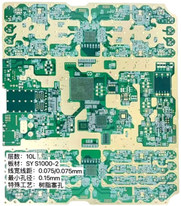
12 to 50+ layers
-
Buried and blind via structures
-
Sub-100 µm line/space geometries
-
Integrated passive components
-
Mixed materials (such as FR4 with PTFE)
-
Controlled impedance and high-speed signal pathways
-
Rigid-flex structures
Their design is not merely about layer count, but also about performance, reliability, and manufacturability under extreme electrical, thermal, and mechanical conditions. The advent of IoT, AI, and edge computing has accelerated the demand for such advanced boards.
Common Difficulties in Manufacturing High-Level PCB Circuit Boards
1. Difficulty in Lamination Process for High-Level PCB Circuit Boards
One of the core complexities of manufacturing High-Level PCB Circuit Boards is the lamination process. Multilayer PCBs require multiple lamination cycles, especially when integrating HDI features like blind and buried vias. Each lamination cycle introduces potential misalignment, resin starvation, voids, or delamination risks.
Solutions:
-
Use low-flow or no-flow prepregs for better interlayer adhesion.
-
Employ laser-assisted registration systems to maintain precision.
-
Adopt high-temperature and high-pressure lamination protocols with real-time monitoring systems.
2. Drilling and Via Challenges in High-Level PCB Circuit Boards
The increasing layer count and tighter spacing make via drilling and metallization increasingly difficult. Microvias and stacked vias require extreme precision and smooth wall plating.
Issues include:
-
Microvia collapse or cracking
-
Void formation during plating
-
Drill wander impacting registration accuracy
Solutions:
-
Use laser drilling for precise microvia formation.
-
Implement plasma desmear processes for better hole cleanliness.
-
Deploy advanced copper plating techniques such as EP (Electroless Plating) or DC Pulse Plating to ensure uniform depositions.
3. Material Compatibility for High-Level PCB Circuit Boards
As designs become more demanding, standard FR4 substrates are no longer sufficient. High-frequency and high-speed requirements demand hybrid materials like Rogers, PTFE, Megtron, and polyimide.
Challenges:
-
CTE (Coefficient of Thermal Expansion) mismatch
-
Poor adhesion between dissimilar materials
-
Material shrinkage during curing
Solutions:
-
Choose material sets with matched CTE values
-
Use press cycles customized to material behavior
-
Partner with experienced suppliers like SQ PCB, who provide material stack-up consultation and design validation support.
4. Fine Line and Space Control for High-Level PCB Circuit Boards
With traces as thin as 40µm or below, etching becomes extremely critical. Overetching can cause open circuits, while underetching leads to shorts.
Issues:
-
Inconsistent trace width
-
Signal integrity degradation
-
Etching undercut
Solutions:
-
Implement laser direct imaging (LDI) systems for accurate photolithography
-
Use automated optical inspection (AOI) at every imaging step
-
Maintain a strict chemical control in etching solutions
5. Impedance Control and Signal Integrity in High-Level PCB Circuit Boards
Maintaining tight impedance values (±5% or better) is essential for signal integrity, especially in RF and high-speed digital applications.
Key Challenges:
-
Variations in dielectric thickness
-
Imprecise trace width control
-
Inconsistent copper surface roughness
Solutions:
-
Use impedance modeling software (such as Polar or Si9000)
-
Ensure controlled roughness copper foil is used (e.g., VLP or HVLP)
-
Conduct TDR (Time Domain Reflectometry) testing for verification
6. Reliability Testing and Quality Assurance of High-Level PCB Circuit Boards
Given their critical application areas, High-Level PCB Circuit Boards must pass rigorous testing.
Tests include:
-
Thermal shock and cycling
-
Solder float and reflow simulation
-
IST (Interconnect Stress Test)
-
X-ray and microsection analysis
✅ Choosing a qualified manufacturer like SQ PCB ensures that every board undergoes stringent QA procedures, including automated inspection, X-ray alignment checks, and thermal stress analysis.
Stack-Up Complexity in High-Level PCB Circuit Boards
As High-Level PCB Circuit Boards reach 20 layers or more, the physical and electrical properties of the stack-up become increasingly difficult to control. Ensuring signal integrity, power delivery stability, and mechanical integrity simultaneously requires deep engineering coordination.
Challenges:
-
Maintaining planarity across multiple dielectric layers
-
Ensuring uniform resin flow to prevent delamination
-
Matching Z-axis expansion rates between core and prepreg materials
-
Managing skewed signal paths across complex reference plane geometries
Solutions:
-
Utilize 3D stack-up modeling tools (e.g., Zuken CR-8000 or Si8000)
-
Adopt symmetric stack-up designs to balance mechanical stress
-
Select high-Tg, low-Dk, low-Df laminates to minimize expansion mismatch
-
Implement press-fit registration systems for exact alignment during lamination
HDI Manufacturing Complexity in High-Level PCB Circuit Boards
High-Level PCB Circuit Boards frequently adopt HDI (High-Density Interconnect) structures to support high-functionality in small form factors. While HDI enables miniaturization, it also introduces layers of complexity in via design, signal routing, and build-up sequencing.
Key Issues:
-
Via-in-pad can cause solder wicking if not properly filled or capped
-
Stacked vias increase risk of delamination if plating is uneven
-
Multiple build-up cycles increase cumulative process variation
-
Difficulty in maintaining impedance and length matching for high-speed signals
Solutions:
-
Use resin-filled and capped vias with vacuum-assisted plating
-
Apply sequential lamination with via stagger strategies
-
Design routing rules to prevent microvia reliability loss due to thermal cycling
-
Perform DFM (Design for Manufacturability) checks early in the design phase
Automated Testing Challenges in High-Level PCB Circuit Boards
Testing complexity increases dramatically with High-Level PCB Circuit Boards, particularly for boards with hundreds of nets, embedded components, and high-speed requirements. Traditional flying-probe testing may not be sufficient due to time constraints and access limitations.
Challenges:
-
Access to internal nets is limited
-
Capacitive testing may give false positives on dense boards
-
Embedded components or shielding make optical inspection harder
-
High-speed nets require advanced signal integrity validation tools
Solutions:
-
Use bed-of-nails fixtures customized for mass testing
-
Combine ICT (In-Circuit Testing) and functional testing
-
Deploy X-ray inspection and microsectioning for internal fault detection
-
Integrate Boundary Scan (JTAG) for complex digital boards
Advanced Equipment Requirements for High-Level PCB Circuit Boards
Conventional PCB equipment often lacks the precision and repeatability required for producing high-end boards. As such, investment in high-end fabrication machinery becomes critical.
Necessary Capabilities:
-
LDI imaging machines for precise fine-line exposure
-
Pulse plating lines to ensure via reliability
-
High-speed AOI systems with 3D profile detection
-
Vacuum lamination presses with temperature and pressure profiling
Thermal Management in High-Level PCB Circuit Boards
Thermal buildup is a serious concern for High-Level PCB Circuit Boards used in high-power applications such as base stations, servers, or electric vehicles.
Problems:
-
Hot spots caused by dense copper areas or stacked vias
-
Outgassing or delamination due to inadequate thermal relief
-
Failure of dielectric material under continuous thermal stress
Solutions:
-
Integrate thermal vias and heatsinks into the stack-up
-
Use ceramic-filled or metal core materials for better heat dissipation
-
Model thermal distribution using FEA simulation tools like Ansys
-
Optimize power plane layout to spread current and heat evenly
Industrial Application-Specific Requirements for High-Level PCB Circuit Boards
Different industries impose distinct performance expectations on High-Level PCB Circuit Boards, often stretching the design and fabrication boundaries.
Aerospace and Military:
-
Must withstand extreme temperature fluctuations and vibration
-
Require MIL-STD-31032 certification
-
Often use polyimide substrates for thermal endurance
Medical Devices:
-
Emphasis on biocompatibility and miniaturization
-
Strict adherence to IPC-6012 Class 3A reliability standards
-
Necessitate cleanroom manufacturing conditions
5G Communication Infrastructure:
-
Demand ultra-low-loss materials
-
Require tight impedance and delay matching
-
Use hybrid stack-ups with PTFE and FR4 in combination
Balancing Manufacturability and Cost in High-Level PCB Circuit Boards
Designers often aim for the best electrical performance, but manufacturing realities impose trade-offs. Overengineering can lead to unsustainable production costs, while underengineering risks performance failure.
Design Choices That Increase Cost:
-
Unnecessarily tight trace/space (e.g., 30μm instead of 50μm)
-
Overuse of stacked microvias when staggered would suffice
-
Blind vias on multiple layers instead of redistributing connections
-
Using exotic materials when high-performance FR4 would suffice
Solutions:
-
Use cost-performance models to simulate electrical gain versus cost increase
-
Implement Design-to-Cost (DTC) methodology in early planning
-
Consider standard panel sizes and standard via types
-
Rely on manufacturers like SQ PCB, who offer value-engineering recommendations without compromising board performance
Conclusion: Solving the Puzzle of High-Level PCB Circuit Boards
Producing High-Level PCB Circuit Boards is not merely a question of stacking more layers—it’s about achieving a synergy between material science, electrical engineering, mechanical precision, and manufacturing excellence.
From multi-stage lamination, micron-level drilling, and HDI routing, to surface finishing, test validation, and global certification, each phase introduces unique challenges. These must be addressed with the right tools, knowledge, and partners.
Companies that attempt to push boundaries must do so with design for reliability, manufacturability, and compliance in mind. Otherwise, the promise of performance can easily be eclipsed by failure in yield, cost, or field reliability.
FAQ: High-Level PCB Circuit Boards
1. What is the difference between rolled copper foil and electrolytic copper foil?
Rolled copper foil is produced by mechanically rolling copper into thin sheets, which offers better surface quality and mechanical strength. Electrolytic copper foil is deposited via an electrolytic process, making it more flexible and cost-effective, though typically rougher in surface finish.
2. How many lamination cycles can a high-level PCB tolerate before failure risk increases?
Generally, up to 3–5 lamination cycles are feasible without serious degradation, but success depends on prepreg type, resin flow behavior, and process controls.
3. Why is laser drilling preferred for microvias in High-Level PCB Circuit Boards?
Laser drilling offers high precision, clean walls, and minimal mechanical stress, which are essential for maintaining interlayer connectivity in HDI designs.
4. Can FR4 be used in high-speed high-level PCBs?
Some high-performance FR4 variants (e.g., low-loss FR4) can be used in moderate-speed applications, but true high-speed designs often require enhanced materials like Megtron6 or Rogers for better electrical properties.
5. What’s the impact of copper surface roughness on high-speed PCB performance?
Higher surface roughness increases signal loss due to skin effect. Using smooth copper foils (HVLP or VLP) reduces insertion loss and improves signal transmission.

- long board pcb
- Flexible PCBs
- Special PCB
- Express Printed Circuit Board
- Pcb Prototype
- LED PCB
- PCB
- Printed Circuit Board
- Pcb meaning
- Pcb manufacturer
- Rigid pcb board
- Rigid Flex PCB
 Quote
Quote
 E-mail