1: Introduction to High Frequency Communication Circuits for High Frequency PCB
1.1 The Role of High Frequency Communication Circuits in Modern Electronics
In the ever-accelerating realm of digital transformation, communication systems are rapidly evolving to support higher bandwidths, greater speed, and more complex data flows. At the heart of these innovations lies a foundational element: High Frequency Communication Circuits. These circuits, operating typically in the gigahertz range, enable reliable and efficient transmission of information over wireless, optical, or wired media.
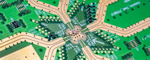
A High Frequency PCB (Printed Circuit Board) is the physical platform that supports these circuits. Unlike traditional PCBs, these boards are engineered with materials and layouts that minimize signal loss, electromagnetic interference, and cross-talk, which are critical considerations at high frequencies. The demand for such technology is evident across applications such as 5G, satellite communication, radar systems, IoT networks, and high-speed computing.
Reflecting on the industry trend, one can see a clear shift from low-speed logic design to RF/microwave-centric circuit architectures. The challenge, however, lies not only in the component design but also in understanding how high-frequency signals behave when routed through complex PCB layers. This duality—between circuit design and physical signal propagation—is where true innovation happens.
1.2 Key Characteristics of High Frequency Communication Circuits
High Frequency Communication Circuits exhibit distinct behaviors that differentiate them from their low-frequency counterparts. Some of the defining characteristics include:
-
Wavelength Sensitivity: At gigahertz-level frequencies, the wavelength becomes comparable to trace lengths on a PCB. As a result, even minor variations in trace geometry or dielectric properties can cause phase shifts, impedance mismatches, and signal reflections.
-
Transmission Line Behavior: Unlike low-frequency circuits where wires act like simple conductors, high-frequency traces must be treated as transmission lines. This introduces concepts such as characteristic impedance, propagation delay, and signal integrity modeling.
-
Electromagnetic Radiation and Crosstalk: These circuits are more prone to EMI and signal coupling due to their shorter rise times and higher energy density in signals. This places strict constraints on trace spacing, layer stacking, and shielding methods.
In my opinion, understanding the nuances of how signal frequency interacts with the physical medium is crucial for mastering high-speed digital design. Too often, engineers underestimate the electromagnetic aspect, treating high-frequency boards as scaled-up versions of regular designs. This is a fundamental mistake.
1.3 Importance of Material Selection in High Frequency Communication Circuits
One of the most influential factors in the performance of High Frequency Communication Circuits is the choice of PCB substrate material. Common FR-4 boards, while cost-effective, are unsuitable for high-frequency use due to high dielectric loss and variable permittivity.
Preferred materials include:
-
PTFE (Teflon): Offers excellent dielectric stability and ultra-low loss, ideal for microwave and RF circuits.
-
Rogers Laminates: Known for precise dielectric properties and compatibility with advanced PCB fabrication processes.
-
Ceramic-Filled Composites: Provide thermal and dimensional stability while maintaining low signal loss.
The dielectric constant (Dk), dissipation factor (Df), and thermal coefficient of Dk are all parameters that directly affect signal integrity at high speeds. These material properties influence everything from impedance control to power handling capability.
From a designer’s standpoint, I believe material selection should be treated as a core design decision rather than a procurement constraint. The temptation to economize on materials often leads to subpar performance in high-frequency applications, and in the long term, can cost more in terms of rework and field failures.
1.4 Interplay Between High Frequency Communication Circuits and PCB Design Rules
The relationship between High Frequency Communication Circuits and the design rules of a high-frequency PCB is deeply intertwined. The layout strategy is no longer just about component placement; it becomes a critical factor in circuit functionality. Important design rules include:
-
Controlled Impedance Routing: Ensures uniform signal propagation and prevents reflection.
-
Differential Pair Matching: Crucial for high-speed serial links, where timing skew must be minimized.
-
Ground Plane Management: A continuous reference plane is essential for return paths, especially in multilayer PCBs.
Another layer of complexity arises when combining analog RF circuits with high-speed digital components, a scenario that is increasingly common in systems like software-defined radios or advanced wireless routers.
High Frequency Communication Circuits
2: Theoretical Principles of High Frequency Communication Circuits in PCB Design
2.1 Fundamental Electromagnetic Theory Behind High Frequency Communication Circuits
To truly comprehend how High Frequency Communication Circuits function within high frequency PCB systems, it’s essential to begin with electromagnetic theory. At lower frequencies, designers often rely on simplified circuit models—resistors, capacitors, inductors—to predict behavior. However, at high frequencies (typically above 500 MHz and into the GHz range), these lumped models break down. Instead, we must treat traces as distributed systems where Maxwell’s equations reign supreme.
Maxwell’s equations describe how electric and magnetic fields propagate, interact with materials, and give rise to electromagnetic waves. In the context of a high frequency PCB, every signal trace effectively becomes a waveguide, governed by the principles of wave propagation. Parameters like propagation velocity, wavelength, and skin depth become critical.
In my view, engineers designing High Frequency Communication Circuits need to develop fluency in field theory—not to the level of writing analytical proofs, but to the extent of developing an intuitive grasp of what the fields are doing in the PCB stack-up. This awareness helps diagnose layout issues, understand EMI sources, and manage coupling.
2.2 The Transmission Line Model in High Frequency Communication Circuits
The concept of a transmission line is pivotal in high frequency communication circuit theory. A transmission line is essentially any pair of conductors (trace and return path) that guides electromagnetic energy from one point to another. In PCB terms, this might be a microstrip or stripline configuration.
Key parameters of a transmission line include:
-
Characteristic Impedance (Z₀): Typically 50Ω or 75Ω, depending on the application. Matching this impedance across the entire signal path is critical to avoid reflections.
-
Propagation Delay: Determined by the dielectric constant and physical length of the line.
-
Reflection Coefficients: Arise when there is an impedance mismatch, causing part of the signal to reflect back toward the source.
-
Signal Attenuation: Due to conductor losses (skin effect) and dielectric losses.
High frequency circuits cannot be understood without modeling their interconnects as transmission lines. Even simple signals like clock pulses or serial data need to be considered as traveling waves.
From a personal design standpoint, I always recommend simulating signal behavior using 2D or 3D field solvers during early stages. This avoids surprises during post-layout verification. Investing time in understanding these physical effects early always pays off in reliability and performance.
2.3 Parasitics and Their Impact on High Frequency Communication Circuits
At high frequencies, parasitic inductance and capacitance play a disproportionate role in altering circuit behavior. A via, which may seem electrically neutral at low frequencies, introduces parasitic inductance and acts as a resonator when transitioning layers. Similarly, even small component pads and trace stubs can become significant sources of reflection or impedance mismatch.
Typical parasitic effects include:
-
Pad Capacitance: Can detune matching networks and alter filter responses.
-
Via Inductance: Affects return current paths and increases loop area.
-
Coupling Capacitance: Between adjacent traces, leading to unwanted signal interference or crosstalk.
Designing High Frequency Communication Circuits requires precise modeling of these parasitics. Tools like S-parameter extraction and full-wave 3D EM solvers help predict and mitigate such behaviors.
Reflecting on my experience, it’s fascinating how small physical features—mere fractions of a millimeter—can make or break signal integrity. Understanding this sensitivity changes the way one approaches layout, component placement, and even stack-up design.
2.4 Frequency-Dependent Behavior of Passive Components in High Frequency Communication Circuits
Resistors, capacitors, and inductors no longer behave ideally at high frequencies. Their impedance becomes a function of frequency due to inherent parasitic elements. For instance:
-
Surface-mount resistors can become inductive at high frequencies.
-
Capacitors exhibit self-resonance, after which they behave inductively.
-
Inductors also reach a self-resonant point where their impedance starts decreasing with frequency.
In high frequency designs, these behaviors can cause unintended circuit detuning or instability. Designers often switch to RF-optimized components—capacitors with low ESL (Equivalent Series Inductance) or inductors specifically designed for GHz frequencies.
Personally, I believe the only way to effectively use passive components in High Frequency Communication Circuits is to study their impedance plots (e.g., using manufacturer-provided SPICE or S2P files) across the operating frequency band. Relying solely on datasheet values at 1 MHz or DC conditions is a common beginner’s mistake.
3: PCB Material Technologies Supporting High Frequency Communication Circuits
3.1 Role of Substrate Materials in High Frequency Communication Circuits
When dealing with High Frequency Communication Circuits, the importance of selecting the right substrate material cannot be overstated. At high frequencies, PCB materials are not just passive insulators—they actively influence signal propagation, attenuation, and overall circuit performance. This makes the dielectric properties of materials a central concern in high-frequency PCB design.
Unlike low-frequency digital boards where standard FR-4 suffices, high-frequency circuits demand materials with tightly controlled dielectric constant (Dk), low dissipation factor (Df), low moisture absorption, and excellent thermal stability. These parameters directly affect the velocity of signal propagation, impedance control, and dielectric losses.
In my design experience, the material decision is not just technical—it’s strategic. Balancing performance with cost and manufacturability is one of the most complex parts of high frequency board planning. Material choice can either elevate the system to meet RF requirements—or completely undermine it.
3.2 Limitations of FR-4 in High Frequency Communication Circuits
FR-4 is the most commonly used PCB substrate in the electronics industry. It is affordable, widely available, and easy to process. However, its performance significantly degrades in High Frequency Communication Circuits due to:
-
High Df (0.02–0.04), leading to high dielectric loss
-
Variable Dk (4.2–4.7) across frequency and temperature ranges
-
Poor impedance control in multilayer stack-ups
-
High moisture absorption, affecting performance in humid environments
FR-4 may still be usable in circuits up to 500 MHz–1 GHz if trace lengths are short and performance demands are relaxed. However, in the gigahertz regime (e.g., 2.4 GHz for Wi-Fi or 28 GHz for 5G mmWave), it introduces too much signal degradation and phase distortion.
For a long time, I attempted to “stretch” FR-4 for RF applications using shielding, signal conditioning, and impedance tuning techniques. Eventually, I realized the better strategy was simply choosing a material optimized for the frequency range I was working in.
3.3 PTFE-Based Materials for High Frequency Communication Circuits
Polytetrafluoroethylene (PTFE), commercially known as Teflon, is one of the most effective substrates for High Frequency Communication Circuits. It offers:
-
Ultra-low Df (~0.0002–0.002)
-
Stable Dk (2.1–2.6) over wide frequency and temperature ranges
-
Excellent chemical resistance and thermal stability
-
High power handling capacity
PTFE laminates are often reinforced with glass or ceramic fillers to improve mechanical strength. These include widely used materials like Rogers RT/duroid, Taconic, and Arlon laminates.
Despite their advantages, PTFE-based materials are more expensive and require special handling during PCB fabrication due to their softness and thermal expansion characteristics. For example, PTFE boards often demand plasma treatment to improve adhesion and more precise etching controls to maintain trace width.
In my professional opinion, if your circuit operates beyond 6 GHz or handles critical RF transmission (e.g., in radar or satellite communications), PTFE laminates should be your default choice. Their performance margins provide design confidence that no layout trickery can substitute for.
3.4 Ceramic-Filled Hydrocarbon Substrates in High Frequency Communication Circuits
A newer class of materials combines ceramic fillers with hydrocarbon resins, offering a middle ground between FR-4 and pure PTFE. These materials aim to improve process compatibility while delivering superior electrical performance. Examples include:
-
Rogers RO4350B and RO4003C
-
Isola Astra MT77
-
Panasonic Megtron series
They exhibit:
-
Low Df (~0.0037–0.0050)
-
Stable Dk (~3.5–3.8)
-
Excellent thermal reliability
-
Processability similar to FR-4
These laminates are popular in automotive radar, 5G base stations, and satellite navigation systems where performance and manufacturability must coexist. They allow manufacturers to produce High Frequency Communication Circuits using traditional fabrication lines, reducing the overall cost of ownership.
In my assessment, ceramic-filled hydrocarbon materials offer the best balance for most commercial RF systems. Unless your design operates above 20 GHz or demands extreme stability, these materials are often the most cost-effective high-performance choice.
3.5 Key Parameters to Evaluate for PCB Materials in High Frequency Communication Circuits
When evaluating materials for High Frequency Communication Circuits, focus on the following technical metrics:
| Parameter | Importance | Typical Good Range |
|---|---|---|
| Dielectric Constant (Dk) | Affects signal speed and impedance | 2.2 – 3.8 (stable with freq/temperature) |
| Dissipation Factor (Df) | Indicates dielectric loss | < 0.005 |
| Moisture Absorption | Affects reliability in humid conditions | < 0.1% |
| Thermal Coefficient of Dk | Stability over temperature | Close to 0 ppm/°C |
| Surface Roughness | Affects conductor loss | < 2 µm preferred |
| Glass Transition Temperature (Tg) | Thermal stability | > 200°C recommended for high-frequency use |
In my opinion, engineers often focus too much on Dk and forget the importance of Df and roughness. At high frequencies, especially over 10 GHz, Df dominates signal loss, and rough copper interfaces can add dB-level degradation.
3.6 Multilayer Stack-Up Design and Lamination Compatibility in High Frequency Communication Circuits
In modern High Frequency Communication Circuits, multilayer boards are common, especially when integrating digital, analog, and RF domains. The choice of materials for different layers must account for:
-
Thermal compatibility to prevent delamination
-
Matching Z-axis expansion to prevent via cracking
-
Compatible lamination cycles to avoid voids or resin starvation
Hybrid stack-ups are often used where high-frequency layers (e.g., Rogers RO4350B) are bonded with FR-4 for power or control planes. This requires bonding films like Rogers 4450F to ensure good adhesion between layers.
This is an area where cross-disciplinary collaboration becomes essential. Material engineers, fabrication partners, and designers must work closely to ensure the chosen materials align in processing as well as in performance. Based on projects I’ve led, early engagement with the PCB fab during stack-up planning prevents 90% of manufacturing issues down the line.
3.7 Environmental Considerations: Moisture, Temperature, and Aging Effects
High Frequency Communication Circuits are vulnerable to environmental degradation. Three major threats are:
-
Moisture Ingress: Increases dielectric constant and loss tangent, detuning circuits.
-
Thermal Cycling: Repeated heating/cooling causes mechanical stress, potentially breaking vias or delaminating layers.
-
Material Aging: Long-term chemical changes can increase loss and shift impedance.
For mission-critical systems (e.g., aerospace or medical), materials with low moisture absorption, high Tg, and proven long-term stability are essential.
Part 4: Layout and Routing Guidelines for High Frequency Communication Circuits
4.1 Importance of PCB Layout in High Frequency Communication Circuits
In High Frequency Communication Circuits, the layout is no longer a passive stage of the design process. It is an active contributor to the electrical behavior of the circuit. At frequencies above 1 GHz, signals behave as electromagnetic waves rather than simple voltage levels. As a result, even the physical geometry of a trace—its length, width, proximity to ground planes, and via transitions—can significantly influence signal quality.
Incorrect layout can result in:
-
Impedance mismatch and reflections
-
Increased electromagnetic interference (EMI)
-
Crosstalk between adjacent lines
-
Ground bounce and return path discontinuities
In my experience, early collaboration between circuit designers and layout engineers is crucial. It’s not enough to just hand over a schematic—one must plan the physical implementation as part of the electrical design. In high frequency design, the line between logical and physical domains is very thin.
4.2 Controlled Impedance Routing in High Frequency Communication Circuits
For High Frequency Communication Circuits, every signal trace must be treated as a transmission line, and its impedance must be controlled with precision—typically 50 ohms for single-ended and 100 ohms for differential pairs. Controlled impedance routing involves:
-
Trace width and spacing: Determined by the PCB stack-up and dielectric properties
-
Distance to reference plane: Essential for maintaining consistent impedance
-
Use of impedance calculators or field solvers: Tools like Polar Si9000 or Altium’s built-in calculators assist in tuning trace geometries
Deviations in impedance cause signal reflections, leading to increased jitter, degraded eye diagrams, and lower signal integrity. A poorly designed trace might reflect a portion of the signal back to the source, causing waveform distortion that no software correction can fix.
From a practical standpoint, I’ve learned that tolerances must be applied not just to dimensions, but also to copper roughness, plating thickness, and manufacturing variations. Including a ±10% impedance margin is standard practice for manufacturability.
4.3 Differential Pair Routing Strategies in High Frequency Communication Circuits
Differential signaling is widely used in High Frequency Communication Circuits, especially in high-speed interfaces like USB 3.x, PCIe, HDMI, LVDS, and Ethernet. In these cases, two complementary signals are routed as a pair. This improves noise immunity and reduces EMI.
Proper differential pair routing requires:
-
Matching trace lengths: To maintain signal timing and avoid skew
-
Consistent spacing: To preserve differential impedance
-
Avoiding stubs: Use back-drilled vias or via-in-pad when necessary
-
Routing on the same layer: To prevent discontinuities in impedance
I’ve observed that designers often underestimate the significance of pair matching, especially in differential clock signals. A skew as small as 10 ps can significantly degrade system performance. Simulating and tuning these pairs during layout is not optional—it’s mandatory.
4.4 Return Path Control in High Frequency Communication Circuits
For every high-speed signal, the return current must flow through a defined low-impedance path, typically a continuous ground plane directly beneath the trace. If the return path is disrupted—for example, by a split plane or via transition without a stitching capacitor—signal integrity suffers.
Good return path practices include:
-
Continuous reference planes beneath all critical signals
-
Avoid crossing plane splits with high-speed signals
-
Use of stitching vias to provide a low-inductance return path near signal vias
-
Capacitive coupling across power/ground boundaries
In high frequency design, current doesn’t take the shortest path—it takes the path of least impedance. This principle reshapes the way we think about ground planes. Personally, I always include ground continuity analysis in my PCB review checklist. Skipping this leads to EMI issues that are very hard to resolve post-fabrication.
4.5 Managing Crosstalk in High Frequency Communication Circuits
Crosstalk occurs when a signal on one trace induces an unwanted signal on a neighboring trace. In High Frequency Communication Circuits, crosstalk can destroy signal fidelity, especially in tightly packed multilayer designs. Types include:
-
Near-end crosstalk (NEXT): Interference seen at the driver end
-
Far-end crosstalk (FEXT): Interference at the receiver end
To minimize crosstalk:
-
Increase spacing between adjacent high-speed signals
-
Use ground traces or guard traces to isolate aggressive lines
-
Avoid parallel routing of critical signals over long distances
-
Route differential pairs closely to reduce the loop area
From my experience, crosstalk is often a “silent killer.” It doesn’t always show up in time-domain signals but manifests in long-term reliability issues like bit errors or random restarts in embedded systems. Pre-layout simulation using 3D field solvers like Ansys HFSS or Keysight ADS can help visualize coupling before it becomes a problem.
4.6 Via Management in High Frequency Communication Circuits
Vias are necessary for layer transitions in multilayer PCBs, but they introduce discontinuities in high-speed signal paths. Each via adds parasitic inductance and capacitance, potentially altering the signal’s characteristic impedance. In High Frequency Communication Circuits, this can lead to:
-
Signal reflections
-
Phase distortion
-
Bandwidth reduction
Best practices include:
-
Minimize the number of vias in high-speed paths
-
Use back-drilling to eliminate unused via stubs
-
Use blind and buried vias to reduce delay
-
Ensure ground vias accompany signal vias for return path continuity
In my work with mmWave designs, I’ve seen systems fail due to un-optimized via transitions. Even when the schematic and layout appear flawless, the via structure can introduce frequency-domain anomalies. This reinforces the importance of full path continuity—not just at DC, but across the RF spectrum.
4.7 Power Delivery and Decoupling in High Frequency Communication Circuits
High-frequency circuits require stable and clean power delivery, which is often overlooked. Voltage transients, ground bounce, and noise coupling are more pronounced at high speeds. Therefore, a power delivery network (PDN) must be carefully engineered.
Design considerations include:
-
Use of power and ground planes for low-impedance power routing
-
Placement of decoupling capacitors close to IC power pins
-
Use of multiple capacitor values (e.g., 0.1 µF, 1 µF, 10 µF) to handle different frequency ranges
-
Avoid narrow traces in power delivery paths
Simulating the PDN impedance using tools like Keysight PIPro or Cadence Sigrity ensures that power integrity is maintained across the target frequency range. Personally, I’ve found that poor PDN design often masquerades as signal integrity problems. This is why I treat PDN verification as an integral part of signal integrity.
Conclusion
Throughout this comprehensive exploration of High Frequency Communication Circuits in the context of High Frequency PCB design, several critical themes have emerged:
-
Fundamental Circuit Principles and Design: The importance of signal integrity, impedance control, and managing parasitic effects cannot be overstated. Every element from trace geometry to component placement impacts the ultimate RF performance.
-
Material Selection and PCB Stackup: Choosing the right substrate materials and copper foil types is crucial for minimizing dielectric and conductor losses, ensuring thermal stability, and maintaining consistent electrical properties over frequency and environmental variations.
-
Thermal Management: As frequencies and power densities increase, managing heat becomes essential not just for reliability but for preserving signal fidelity. Techniques like thermal vias, heat sinks, and advanced simulation are indispensable.
-
Testing and Validation: Employing advanced tools such as VNAs, TDRs, BER testers, and environmental chambers ensures that designs translate effectively from theory to real-world applications.
-
System Integration Challenges: Integrating high-frequency circuits within complex, multi-domain systems requires careful partitioning, shielding, and interface management to mitigate EMI, ensure timing synchronization, and maintain signal integrity.
-
Future Trends and Innovations: Emerging areas like mmWave and terahertz frequencies, photonic integration, AI-assisted design, advanced substrates, and additive manufacturing are reshaping the design landscape.
Designing High Frequency Communication Circuits for PCBs requires a multidisciplinary approach, combining electromagnetic theory, material science, and advanced simulation tools. As wireless technology evolves, engineers must adapt to new challenges in signal integrity, miniaturization, and power efficiency.
By mastering these principles, designers can push the boundaries of high-frequency electronics, enabling next-generation communication systems.

- long board pcb
- Flexible PCBs
- Special PCB
- Express Printed Circuit Board
- Pcb Prototype
- LED PCB
- PCB
- Printed Circuit Board
- Pcb meaning
- Pcb manufacturer
- Rigid pcb board
- Rigid Flex PCB
 Quote
Quote
 E-mail