1. Introduction
In the world of printed circuit board (PCB) manufacturing, E-Test, short for Electrical Test, is a critical quality control process. It ensures the functionality and reliability of a PCB by identifying defects such as short circuits, open circuits, and other electrical failures before the final assembly. With the increasing complexity of modern PCBs, E-Test plays a vital role in maintaining performance standards and reducing production costs.
In the ever-evolving world of electronics, Printed Circuit Boards (PCBs) serve as the backbone of modern devices, from smartphones and computers to aerospace and medical equipment. As these devices become more complex and miniaturized, ensuring the functionality and reliability of PCBs becomes increasingly critical. This is where E-Test (Electrical Test) plays a vital role.
1.1 Understanding the Role of Electrical Testing in PCB Manufacturing
E-Testing refers to the process of verifying the electrical performance and integrity of a PCB by identifying open circuits, short circuits, and other defects that may compromise functionality. This testing process ensures that the PCB meets design specifications before moving on to assembly and final product integration. Without E-Test, manufacturers risk producing faulty boards, leading to product failures, increased costs, and damaged reputations.
1.2 Evolution of E-Test Technology
Over the past few decades, Electrical Testing methodologies have advanced significantly. Traditional manual testing methods have been replaced by automated systems that leverage flying probe testers, bed-of-nails fixtures, and advanced software solutions. These innovations allow for high-speed, high-accuracy testing of both simple single-layer PCBs and complex multi-layer, high-density boards.
- Flying Probe Testers: Suitable for low to medium-volume production, flying probe testers use movable probes to access test points on the PCB without the need for custom fixtures. This method is flexible and cost-effective for prototyping and small batch testing.
- Bed-of-Nails Testers: Ideal for high-volume production, this method utilizes a custom fixture with fixed probes that make contact with specific test points on the PCB. It offers faster testing speeds but requires significant upfront investment in fixture design.
1.3 Importance of Electrical Testing in Quality Control
The primary objective of Electrical Testing is to detect manufacturing defects that can lead to product failures. These defects can stem from various sources, including:
- Material Issues: Poor-quality substrates, conductive traces, or solder masks.
- Manufacturing Errors: Incorrect drilling, misaligned layers, or insufficient copper plating.
- Environmental Factors: Thermal stress, humidity, and contamination during the production process.
By identifying these issues early in the manufacturing process, Electrical Testing prevents defective boards from progressing to the assembly stage, reducing rework costs and improving overall product reliability.
1.4 The Impact of PCB Complexity on E-Testing Requirements
As technology advances, PCBs are becoming more complex, featuring finer traces, smaller vias, and higher layer counts. High-speed digital circuits, RF/microwave designs, and flexible PCBs present unique testing challenges that require more sophisticated Electrical Testing solutions.
For example, high-frequency PCBs used in 5G infrastructure demand precise impedance control and signal integrity verification. In such cases, Electrical Testing must not only check for electrical continuity but also evaluate impedance matching and crosstalk.
1.5 Regulatory and Industry Standards
Compliance with international standards is another critical aspect of Electrical Testing. Organizations like the IPC (Association Connecting Electronics Industries) and ISO (International Organization for Standardization) establish guidelines for PCB quality and testing procedures. Adhering to these standards ensures product reliability, reduces liability risks, and enhances customer trust.
Key standards include:
- IPC-6012: Qualification and Performance Specification for Rigid Printed Boards
- IPC-9252: Electrical Test Guidelines for Bare Printed Boards
- ISO 9001: Quality Management Systems
1.6 The Role of Automation and Data Analytics in E-Test
Modern E-Test systems are increasingly integrating automation and data analytics to enhance testing efficiency and accuracy. Automated Optical Inspection (AOI) and X-ray Inspection (AXI) complement traditional electrical tests, allowing for the detection of hidden defects and material inconsistencies.
Additionally, real-time data analytics platforms enable manufacturers to monitor test results, identify trends, and implement continuous improvement strategies. By leveraging machine learning algorithms, manufacturers can predict failure patterns and optimize production processes.
1.7 Addressing Challenges in E-Test Implementation
While E-Test is essential for quality assurance, it also presents certain challenges, such as:
- Cost Management: High-volume testing can be expensive due to fixture costs and equipment maintenance.
- Time Constraints: Rapid testing is crucial for meeting tight production deadlines.
- Compatibility Issues: Testing high-speed and flexible PCBs requires specialized equipment and expertise.
By investing in advanced testing technologies and skilled personnel, manufacturers can overcome these challenges and achieve higher yields and reliability.
1.8 Future Trends and Innovations in E-Test
The future of E-Test is shaped by emerging technologies, including:
- AI-Powered Defect Detection: Machine learning algorithms can analyze test data and identify subtle defect patterns.
- Non-Destructive Testing (NDT): Advanced imaging techniques like infrared thermography and ultrasonic inspection allow for defect detection without damaging the board.
- Cloud-Based Testing Platforms: Real-time data sharing and remote monitoring enhance collaboration and efficiency.
1.9 Conclusion of the Introduction
In summary, Electrical Testing is a critical component of the PCB manufacturing process, ensuring product quality, reliability, and compliance with industry standards. As the electronics industry continues to evolve, Electrical Testing technologies must adapt to handle increasingly complex designs and meet the demands of emerging applications.
E-Test
2. The Importance of E-Test in PCB Production
2.1 Ensuring Circuit Integrity
E-Test verifies that all electrical pathways function as intended, preventing faulty connections and ensuring signal integrity. This step is crucial, especially for high-density and multi-layer PCBs.
2.2 Detecting Manufacturing Defects
Common defects like solder bridges, broken traces, and misaligned vias can be identified through Electrical Testing, allowing manufacturers to address these issues before mass production.
2.3 Reducing Production Costs
By catching defects early in the process, Electrical Testing minimizes the risk of product recalls, reducing waste and saving both time and resources.
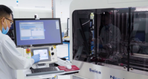
3. E-Test Methods
3.1 Flying Probe Testing
This method utilizes movable probes to test electrical connections without the need for a custom test fixture. It is ideal for low-volume production and prototype testing.
3.2 Bed of Nails Testing
A fixed fixture with numerous pins is used to simultaneously test multiple points on the PCB. This method is more efficient for high-volume production.
3.3 Resistance and Continuity Testing
E-Test measures the resistance between different points to detect open circuits and ensures continuous conductivity.
4. Key Parameters in E-Test
4.1 Isolation Resistance
Verifies that there are no unintended connections between different conductive paths.
4.2 Continuity Check
Ensures that each intended connection is intact and functions as expected.
4.3 Voltage and Current Testing
Confirms that the PCB can handle the specified voltage and current levels without failure.
5. Challenges in E-Test Implementation
5.1 High-Density PCB Complexity
With the miniaturization of electronic components, testing intricate designs becomes increasingly difficult.
5.2 Test Point Accessibility
Ensuring all critical points are accessible for probing can be challenging, especially in multi-layer PCBs.
5.3 Cost and Time Constraints
Balancing thorough testing with production deadlines and budget limitations is a common challenge in the industry.
6. Advanced Technologies in E-Test
6.1 Automated Optical Inspection (AOI) Integration
Combining E-Test with AOI systems improves defect detection accuracy and speeds up the testing process.
6.2 Artificial Intelligence (AI) and Machine Learning
AI-driven E-Test systems can analyze large datasets and identify subtle defects that traditional methods might miss.
6.3 High-Frequency Signal Testing
Advanced E-Test techniques can evaluate the performance of PCBs designed for high-speed communication and RF applications.
7. Best Practices for Effective E-Test Implementation
- Designing PCBs with accessible test points.
- Regular calibration of testing equipment.
- Integrating E-Test early in the manufacturing process.
- Continuous monitoring and data analysis for process improvement.
8. Future Trends in E-Test for PCB Manufacturing
8.1 Enhanced Automation
Fully automated E-Test systems will streamline testing processes and reduce human error.
8.2 Real-Time Data Analytics
Cloud-based platforms will enable real-time monitoring and predictive maintenance.
8.3 Green Testing Solutions
Eco-friendly E-Test methods will reduce energy consumption and material waste.
9. Conclusion: The Future of E-Test in PCB Manufacturing
As the electronics industry advances, E-Test (Electrical Test) remains a cornerstone of quality assurance in PCB manufacturing. The continuous evolution of PCB designs, from single-layer boards to complex multi-layer and high-frequency circuits, demands increasingly sophisticated testing methodologies.
9.1 The Growing Need for Precision and Accuracy
With the rise of 5G technology, IoT devices, and advanced automotive electronics, the demand for high-speed, high-frequency PCBs has surged. These applications require ultra-precise testing to detect minute defects that could compromise performance. Traditional E-Test methods, such as flying probe and bed-of-nails testing, must adapt to handle higher density components and finer traces.
9.2 Integration of Automation and AI
Automation is transforming E-Test processes by reducing human error and increasing efficiency. AI-driven analysis tools can quickly detect patterns in test data, identify potential failure points, and predict manufacturing defects. This proactive approach allows manufacturers to implement corrective actions earlier in the production cycle, significantly reducing scrap rates and improving yield.
9.3 Enhanced Testing for High-Frequency and RF Circuits
High-frequency PCBs, used in telecommunications and radar systems, require specialized E-Testing procedures to measure signal integrity and impedance. Advanced tools like time-domain reflectometers (TDR) and vector network analyzers (VNA) are becoming essential for evaluating the electrical performance of these boards.
9.4 Addressing Environmental and Sustainability Concerns
As the electronics industry moves toward eco-friendly manufacturing practices, E-Testing systems are also evolving to minimize energy consumption and reduce waste. Non-destructive testing methods, such as X-ray inspection and thermal imaging, allow for defect detection without damaging the board, thereby reducing material loss.
9.5 Real-Time Data Analytics and Remote Monitoring
Cloud-based E-Test platforms enable real-time data collection and analysis from multiple manufacturing sites. This centralized approach allows quality control teams to monitor production performance globally, identify trends, and implement corrective actions swiftly. Additionally, remote monitoring capabilities enhance collaboration between design engineers and production teams, leading to faster product development cycles.
9.6 Compliance with Industry Standards and Regulations
Strict regulatory standards, such as IPC-A-600 and ISO 9001, require thorough E-Testing procedures to ensure PCB quality and reliability. Compliance with these standards not only enhances product performance but also builds customer trust and reduces liability risks.
9.7 Future Innovations in E-Test Technologies
- Flexible and Stretchable PCB Testing: As wearable electronics and flexible circuits gain popularity, E-Testing systems must adapt to handle these unique substrates. New probe designs and flexible fixturing solutions are being developed to accommodate bending and stretching during testing.
- Quantum Sensing for Ultra-High Precision Testing: Quantum sensors, which can detect minute changes in magnetic and electric fields, are being explored for high-precision E-Test applications. These sensors can identify sub-micron defects that traditional methods might miss.
- Blockchain Integration for Traceability: Incorporating blockchain technology into E-Testing data management systems can enhance traceability and security, ensuring that test results are tamper-proof and easily accessible throughout the supply chain.
9.8 The Road Ahead: Continuous Improvement and Adaptation
To stay competitive in the rapidly evolving electronics market, PCB manufacturers must continuously invest in advanced E-Testing technologies and skilled personnel. By adopting a holistic approach that combines automation, AI-driven analytics, and sustainable practices, manufacturers can achieve higher yields, reduce costs, and deliver superior products to customers.

- long board pcb
- Flexible PCBs
- Special PCB
- Express Printed Circuit Board
- Pcb Prototype
- LED PCB
- PCB
- Printed Circuit Board
- Pcb meaning
- Pcb manufacturer
- Rigid pcb board
- Rigid Flex PCB
 Quote
Quote
 E-mail