How to Do a PCB from PCB Schematic: Imagine holding a completed electronic device in your hands. Its precision, reliability, and seamless operation are a testament to one key process—PCB design. But before any device comes to life, it starts with a vision sketched into a PCB schematic. That schematic is the blueprint, the roadmap, and the DNA of your circuit board.
The challenge? Translating that intricate web of connections into a functional printed circuit board (PCB). This process isn’t just technical; it’s a craft. It requires foresight, creativity, and meticulous attention to detail. Whether you’re working on a compact prototype PCB board or designing for mass production, the journey from schematic to PCB is where ideas transform into innovation.
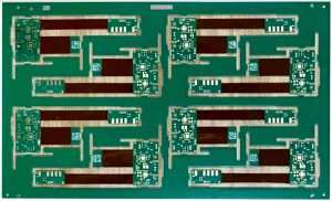
PCB Schematic
How to Do a PCB from PCB Schematic, Why PCB Schematic is Only the Beginning
The PCB schematic is like the script for a play—it defines the roles but doesn’t build the stage. A PCB board is the stage where every component plays its part. From signal routing to selecting the right PCB board materials, the process requires a balance of art and science.
Skip a critical step, and the entire system could fail. Misplace a trace, and you might face noise interference or a short circuit. That’s why understanding how to correctly transform a schematic into a PCB is vital. It’s not just about connecting the dots; it’s about building a reliable foundation for your project.
The Stakes Are High: Getting It Right
The journey from a PCB schematic to a fully functional PCB is filled with critical decisions, each of which can significantly affect your project’s outcome. Every trace, material choice, and layout decision plays a vital role in determining the board’s success. Here’s a deeper dive into how these factors impact your design:
1. Performance: The Lifeblood of Your Circuit
Performance is the essence of any PCB. A single error in trace width or an ill-conceived layout can cascade into serious inefficiencies, signal integrity issues, or electromagnetic interference (EMI).
- Trace Width and Spacing: Too narrow a trace can lead to overheating, especially in high-current circuits. Too wide, and you may run out of space for other components.
- Signal Integrity: Poorly routed traces can introduce crosstalk and EMI, degrading the quality of high-speed signals. Ground planes and shielding can mitigate these issues but must be designed with precision.
- Thermal Management: Heat buildup is a common challenge in compact designs. If your layout doesn’t account for proper heat dissipation, performance can degrade, leading to failure over time.
2. Durability: Building for the Long Haul
Durability isn’t just about physical strength; it’s about ensuring the board withstands environmental stresses and operational demands over time.
- PCB Thickness: Choosing the right board thickness is crucial. A thin board may flex and crack under mechanical stress, while an overly thick board can increase costs unnecessarily.
- Materials: The choice of PCB board materials determines its resistance to heat, moisture, and wear. For example, FR4 is a versatile and widely used material, but for high-frequency or high-temperature applications, specialized substrates like Rogers laminates or metal cores may be more appropriate.
- Environmental Protection: Coatings like solder masks and conformal coatings protect the board from environmental elements like humidity, dust, and corrosive chemicals, enhancing durability.
3. Cost: Balancing Budget and Quality
Cost considerations start early in the design process and can have ripple effects across the entire PCB board manufacturing cycle.
- Error Prevention: Mistakes in the layout stage can lead to costly reworks or delays in production. A poorly planned design might require changes in component placement or even an entirely new schematic.
- Material Costs: Higher-quality materials often come with higher upfront costs, but they can reduce failure rates and extend the product’s lifespan, saving money in the long run.
- Optimization: Efficient layouts can minimize board size, reducing material usage and manufacturing costs. Balancing compactness with functionality is an art that requires a deep understanding of design constraints.
4. Manufacturability: Streamlining the Process
- Design for Manufacturability (DFM): Ensure your design aligns with the capabilities of your chosen manufacturer. Factors like minimum trace width, hole sizes, and layer stack-up must conform to their specifications.
- Prototyping: Before committing to mass production, creating a prototype PCB board is invaluable for testing and validating your design. Prototypes help catch errors early, saving time and money.
- Assembly Considerations: Component placement and orientation directly impact assembly efficiency. Proper spacing and accessible soldering points can streamline the process, avoiding unnecessary delays or complications.
Getting It Right: Key Strategies
Success lies in preparation and attention to detail. Here’s how to set yourself up for a smooth and efficient process:
- Collaborate with Manufacturers: Work closely with your PCB manufacturer to understand their capabilities and limitations.
- Simulate and Validate: Use simulation tools to test your design for potential electrical, thermal, or mechanical issues before moving to production.
- Document Thoroughly: Provide detailed documentation, including design files, assembly drawings, and a bill of materials (BOM), to avoid miscommunication during production.
The Power of Preparation
Before diving into the design software or selecting your blank PCB board, it’s critical to ask:
- What are the design constraints? Space, cost, and thermal considerations all play a role.
- What’s the intended application? Will the board operate in extreme conditions or a controlled environment?
- What materials will you use? Different PCB board materials offer varying benefits in terms of conductivity, strength, and heat resistance.
Answering these questions ensures you’re not just building a PCB but creating a solution tailored to your needs.
The Transformation: From Schematic to PCB
Turning a PCB schematic into a physical board isn’t just a technical task; it’s a transformation. It’s where theory meets practice, where potential becomes tangible. This is the stage where every line, node, and component placement matters. Done right, it’s the foundation of every reliable electronic device you’ve ever used.
By following a methodical process and keeping the final application in mind, you can create a PCB that’s not just functional but exceptional. Whether you’re crafting a prototype PCB board to test a concept or designing a high-performance product for the market, this guide will equip you with the steps and strategies to succeed.
In the following sections, we’ll break down this process into actionable steps, ensuring you’re equipped to handle every aspect of PCB creation with confidence. Stay focused, and let’s dive into the intricacies of PCB schematic transformation.
our linken sqpcb.com

- long board pcb
- Flexible PCBs
- Special PCB
- Express Printed Circuit Board
- Pcb Prototype
- LED PCB
- PCB
- Printed Circuit Board
- Pcb meaning
- Pcb manufacturer
- Rigid pcb board
- Rigid Flex PCB
 Quote
Quote
 E-mail