1. Introduction to Copper’s Effective Permittivity in PCB Design
In modern high-speed PCB design, the performance of circuits is no longer solely determined by layout geometry or component placement. One critical factor that often receives less attention—but has a profound effect on signal integrity—is Copper’s Effective Permittivity. This property defines how copper interacts with the dielectric materials in a PCB and directly influences signal propagation, impedance, and timing across the board. Understanding Copper’s Effective Permittivity is essential for designers aiming to maintain reliable high-frequency performance in applications such as 5G communications, high-speed computing, and advanced automotive electronics.
Copper’s Effective Permittivity is a measure of the apparent permittivity of the PCB structure, as “seen” by high-frequency signals traveling through copper traces. While the nominal permittivity of the substrate material is important, the presence of copper layers modifies the electromagnetic environment, effectively altering the dielectric constant experienced by the signals. In practical terms, this means that a PCB with the same substrate but different copper configurations may exhibit different signal delays, impedance characteristics, and crosstalk behavior.
From a design perspective, ignoring the effects of Copper’s Effective Permittivity can lead to subtle but serious issues such as skew between differential pairs, reflections at impedance mismatches, and even data corruption in high-speed serial links. Conversely, careful consideration of this parameter allows engineers to predict and mitigate signal integrity issues before fabrication, reducing the risk of costly revisions.
Moreover, Copper’s Effective Permittivity plays a role in thermal management and mechanical stability. Copper layers not only conduct electrical signals but also distribute heat, impacting the performance of both the dielectric and the components mounted on the PCB. High-speed boards generate localized hot spots; the effective permittivity can influence how these thermal variations affect the dielectric properties and, consequently, the signal propagation.
My analysis: While traditional PCB design has focused on trace width, spacing, and substrate choice, the role of copper’s permittivity is often underestimated. For next-generation high-speed applications, integrating Copper’s Effective Permittivity into simulation models and layout considerations is no longer optional—it’s a necessity. By proactively optimizing copper layer configurations, designers can achieve superior signal integrity and reduce post-fabrication tuning.
In upcoming sections, we will explore the properties and characteristics of Copper’s Effective Permittivity, how it affects signal integrity, its advantages, and practical strategies to optimize PCB performance. We will also highlight real-world case studies, including boards manufactured by SQ PCB, which exemplify the benefits of thoughtful copper permittivity management.
Copper’s Effective Permittivity
2. Understanding Copper’s Effective Permittivity: Properties and Characteristics
Copper’s Effective Permittivity is a critical electrical property that quantifies the interaction between copper layers and the surrounding dielectric in a PCB. It differs from the intrinsic permittivity of the substrate material because the presence of copper modifies the electric field distribution. Understanding this concept requires examining several aspects, including its definition, influencing factors, frequency dependence, and measurement methods.
2.1 Definition and Concept
In essence, Copper’s Effective Permittivity is the apparent dielectric constant that a signal experiences when traveling through a copper trace over a PCB substrate. Unlike the substrate permittivity (often denoted as ε_r), which is a fixed material property, effective permittivity considers:
-
The geometry and thickness of copper traces
-
The configuration of multiple copper layers (signal, ground, and power planes)
-
The separation between traces and planes
-
The operating frequency of the signals
This makes effective permittivity a more practical and accurate parameter for high-speed PCB design. For example, a tightly coupled microstrip line will exhibit a higher effective permittivity than a loosely spaced trace due to increased field interaction with the dielectric.
2.2 Factors Influencing Copper’s Effective Permittivity
-
Copper Layer Thickness
Thicker copper can slightly reduce effective permittivity because it confines the electric field closer to the trace, decreasing the relative influence of the substrate. -
Copper Surface Roughness
Rolled copper foil generally has a smoother surface, which minimizes high-frequency signal scattering. In contrast, electrolytic copper foil can introduce microscopic roughness, affecting the effective permittivity and causing subtle impedance variations. -
Dielectric Thickness and Type
While copper dominates the electromagnetic environment near the trace, the substrate’s dielectric constant and thickness still significantly impact effective permittivity. High-k substrates result in higher effective permittivity, which can slow down signal propagation. -
Trace Geometry and Layout
Wider traces and closely spaced differential pairs increase coupling to the ground plane and between traces, altering the effective permittivity experienced by the signal. -
Frequency Dependence
At high frequencies, skin effect confines the signal to the outer layers of copper. This changes the field distribution and modifies effective permittivity, making accurate modeling essential for multi-GHz designs.
2.3 Advantages of Understanding Copper’s Effective Permittivity
Accurate knowledge of Copper’s Effective Permittivity enables designers to:
-
Predict propagation delay and adjust trace lengths for signal synchronization
-
Maintain controlled impedance for high-speed differential pairs
-
Reduce crosstalk and unwanted electromagnetic interference
-
Improve simulation accuracy in tools like HFSS, CST, or SIwave
By carefully selecting copper foil type, trace geometry, and substrate properties, engineers can optimize effective permittivity to achieve superior PCB performance.
2.4 Measurement and Simulation Techniques
Effective permittivity can be measured or estimated using several approaches:
-
Time-Domain Reflectometry (TDR): Measures impedance discontinuities and allows extraction of effective permittivity along transmission lines.
-
Vector Network Analyzer (VNA): Frequency-domain measurement to evaluate dielectric properties and loss tangent.
-
Electromagnetic Simulation: Modern EDA tools model copper and dielectric interactions to compute effective permittivity and predict signal behavior before fabrication.
By integrating these measurements early in the design process, designers minimize costly iterations and improve overall board reliability.
My Analysis: Understanding Copper’s Effective Permittivity is not just academic—it is a practical necessity in high-speed PCB design. In my experience, many design teams overlook this factor, focusing solely on trace width or substrate choice. However, subtle variations in copper properties or layer configuration can drastically affect signal integrity, especially at frequencies above 5 GHz. Using precise simulations, validated by measurement, is the best approach for future-proof PCB design.
In the next section, we will examine how Copper’s Effective Permittivity influences signal integrity in high-speed PCBs, highlighting real-world implications for timing, reflections, and differential pair performance.
3. How Copper’s Effective Permittivity Influences Signal Integrity in High-Speed PCBs
In high-speed PCB design, maintaining signal integrity is a critical challenge. As signal frequencies increase, even minor variations in Copper’s Effective Permittivity can have significant impacts on propagation, impedance, and timing. This section explores how this property directly affects the electrical behavior of signals and what designers can do to manage these effects.
3.1 Signal Propagation and Delay
Signal speed in a PCB trace is determined by the effective permittivity of the surrounding medium. The relationship is described by:
v=cεeffv = \frac{c}{\sqrt{\varepsilon_\text{eff}}}
where vv is the signal velocity, cc is the speed of light in vacuum, and εeff\varepsilon_\text{eff} is the Copper’s Effective Permittivity.
A higher effective permittivity slows signal propagation, increasing delay across the trace. In differential or parallel bus architectures, unequal effective permittivity between traces can lead to skew, causing timing mismatches that may corrupt data or reduce operational reliability. Designers must carefully account for this by adjusting trace lengths or selecting copper and dielectric materials to balance signal speed.
3.2 Impedance Control
Controlled impedance is critical for high-speed signals, especially in multi-GHz designs. The characteristic impedance Z0Z_0 of a microstrip or stripline is influenced by effective permittivity:
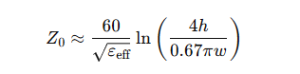
where hh is the dielectric thickness and ww is the trace width. Small changes in effective permittivity can alter impedance, leading to reflections and signal degradation. For instance, using a rough copper surface or inconsistent layer spacing can inadvertently increase effective permittivity, creating impedance mismatch points along high-speed traces.
3.3 Crosstalk and Electromagnetic Interference (EMI)
Copper’s Effective Permittivity influences the coupling between adjacent traces. Higher effective permittivity increases the electromagnetic field concentration within the substrate, which can:
-
Increase near-end and far-end crosstalk between signal lines
-
Alter the effectiveness of ground planes in shielding high-speed signals
-
Make the PCB more sensitive to external EMI sources
By carefully choosing copper foil type, trace width, and layer stacking, designers can optimize effective permittivity to minimize unwanted coupling and improve overall signal fidelity.
3.4 High-Frequency Behavior and Skin Effect
At high frequencies, the skin effect confines current to the outer layers of copper traces. This phenomenon changes the interaction between the copper and the dielectric, effectively modifying Copper’s Effective Permittivity. If not properly accounted for, designers may observe:
-
Unexpected impedance variations
-
Signal attenuation over long traces
-
Frequency-dependent delays that impact multi-GHz data channels
Advanced simulation tools can model these frequency-dependent effects, allowing engineers to predict and correct potential signal integrity problems before fabrication.
3.5 Practical Recommendations
-
Material Selection: Choose copper foils with smooth surfaces (e.g., rolled copper) for high-frequency applications to reduce variation in effective permittivity.
-
Layer Design: Optimize copper plane thickness and trace spacing to maintain uniform effective permittivity across the PCB.
-
Simulation and Measurement: Use TDR and VNA measurements to validate effective permittivity models in prototypes.
-
Manufacturer Collaboration: Working with reliable PCB suppliers like SQ PCB ensures that copper and substrate properties meet design specifications, reducing post-production tuning.
My Analysis: The influence of Copper’s Effective Permittivity on signal integrity is subtle but crucial. Designers often underestimate its impact until signals fail in high-speed prototypes. From my perspective, integrating this property into early-stage design decisions—especially in conjunction with accurate simulation and high-quality copper foils—is the key to achieving reliable, high-performance PCBs.
4. Advantages of Copper’s Effective Permittivity for PCB Performance
While Copper’s Effective Permittivity is often discussed in the context of signal integrity, its benefits extend across multiple dimensions of PCB performance, including thermal management, electrical reliability, and mechanical stability. Proper understanding and optimization of this property allow designers to build boards that are both high-performing and durable.
4.1 Electrical Performance Advantages
Copper’s Effective Permittivity directly impacts:
-
Signal propagation consistency: Uniform effective permittivity ensures predictable signal velocity, reducing skew between differential pairs and enhancing timing accuracy.
-
Controlled impedance: Optimized copper and dielectric interactions help maintain precise impedance, minimizing reflections and improving signal fidelity.
-
Crosstalk reduction: Effective permittivity management reduces unwanted electromagnetic coupling between traces, critical in high-speed data applications.
By leveraging these electrical benefits, designers can achieve superior performance in applications such as high-frequency RF circuits, multi-Gbps data links, and advanced computing boards.
4.2 Thermal Management Benefits
Copper not only carries electrical signals but also acts as an effective heat conductor. Copper’s Effective Permittivity plays an indirect role in thermal performance:
-
Uniform field distribution: Reduces hotspots and uneven dielectric heating, maintaining consistent board characteristics.
-
Enhanced reliability: Lower temperature gradients reduce thermal stress on traces and components, prolonging operational life.
-
Improved power handling: Optimized copper layout and effective permittivity ensure that high-current paths are stable and thermally efficient.
This makes effective permittivity optimization particularly important in power-intensive boards, such as automotive electronics and high-performance computing modules.
4.3 Mechanical and Manufacturing Advantages
Understanding and managing Copper’s Effective Permittivity also supports mechanical reliability:
-
Layer integrity: Balanced copper and dielectric interactions reduce the risk of warping or delamination.
-
Consistent dielectric behavior: Uniform effective permittivity across the board ensures that mechanical stresses do not introduce performance variability.
-
Simplified fabrication: Manufacturers can predict and control trace performance more accurately, reducing iterations and production costs.
4.4 Application-Specific Benefits
In practice, leveraging Copper’s Effective Permittivity provides measurable improvements:
-
High-speed serial interfaces (e.g., PCIe, USB4) achieve better eye-diagram performance.
-
RF and microwave boards maintain stable impedance across frequency ranges.
-
Complex multi-layer PCBs, especially those produced by reliable manufacturers like SQ PCB, show fewer signal integrity issues and require less post-production tuning.
4.5 Summary of Advantages
By carefully designing around Copper’s Effective Permittivity, engineers can:
-
Achieve predictable signal propagation and controlled impedance.
-
Reduce crosstalk and EMI susceptibility.
-
Improve thermal distribution and board reliability.
-
Minimize mechanical stress and maintain layer integrity.
-
Reduce prototype iterations, saving time and cost.
My Analysis: Copper’s Effective Permittivity is a key enabler of modern high-speed PCB performance. From my experience, boards that intentionally account for this property perform consistently better in both laboratory and field testing. While it may seem like a subtle factor compared to trace width or dielectric choice, ignoring it can lead to repeated design failures, especially in multi-GHz systems. Selecting high-quality copper foils, simulating effective permittivity, and collaborating with experienced PCB manufacturers like SQ PCB are critical steps toward optimal results.
5. Design Considerations When Optimizing Copper’s Effective Permittivity
High-speed PCB design is a delicate balance between material selection, trace geometry, and layer configuration. Effective management of Copper’s Effective Permittivity can make the difference between a reliable board and one plagued with signal integrity issues. In this section, we explore actionable strategies and best practices for optimizing this crucial property.
5.1 Material Selection
Selecting the right copper and dielectric materials is the foundation of effective permittivity management:
-
Copper foil type: Rolled copper foil has a smoother surface, leading to lower high-frequency signal scattering. Electrolytic copper foil is more flexible and cost-effective but may slightly increase effective permittivity due to surface roughness.
-
Dielectric materials: Choosing low-loss, stable dielectric substrates (e.g., FR-4 with controlled Dk, Rogers materials) ensures predictable effective permittivity over temperature and frequency ranges.
-
Copper-to-dielectric ratio: The relative thickness of copper to the dielectric layer directly influences field distribution and, consequently, effective permittivity.
5.2 Layer Stack-Up and Trace Configuration
The arrangement of copper layers significantly affects effective permittivity:
-
Microstrip vs stripline: Stripline configurations, where traces are sandwiched between copper planes, usually exhibit higher effective permittivity and better impedance control. Microstrip traces, exposed to air, have lower effective permittivity but are more susceptible to external noise.
-
Layer symmetry: Maintaining symmetrical stack-ups minimizes skew between differential pairs and reduces mechanical stress that could alter permittivity.
-
Trace width and spacing: Wider traces increase coupling with ground planes, raising effective permittivity. Proper spacing between signal lines prevents unwanted crosstalk.
5.3 High-Frequency Considerations
At frequencies above a few GHz, signal behavior becomes more sensitive to variations in effective permittivity:
-
Skin effect: Signal current is confined to the outer layer of copper, changing the effective field distribution.
-
Dielectric dispersion: Permittivity may vary slightly with frequency; selecting materials with stable Dk values across operating ranges is essential.
-
Simulation validation: Tools like HFSS, CST, or Keysight ADS allow designers to simulate these effects, enabling accurate prediction of signal propagation and impedance.
5.4 Practical Design Guidelines
-
Plan for controlled impedance: Use simulation tools and validate with TDR measurements to account for effective permittivity variations.
-
Consider copper roughness: For high-speed signals, prefer smooth rolled copper foils to minimize signal loss and impedance deviations.
-
Optimize layer thickness: Balance copper and dielectric thickness to achieve desired effective permittivity without compromising thermal performance.
-
Collaborate with manufacturers: Engage experienced PCB suppliers such as SQ PCB to ensure copper and dielectric materials meet precise specifications.
-
Prototype and measure: Build small-scale prototypes to verify effective permittivity assumptions before full production.
5.5 My Analysis
From my experience, many engineers overlook effective permittivity until issues arise in prototypes or production boards. However, integrating permittivity considerations early in the design process drastically reduces iteration cycles, improves signal integrity, and ensures reliable high-speed operation. Effective permittivity should be treated as a design parameter, not just a material property, with decisions informed by both simulation and real-world measurements.
6. Material Selection: Copper Foil Types and Copper’s Effective Permittivity
The choice of copper foil is a critical factor in high-speed PCB design, as it directly influences Copper’s Effective Permittivity, signal integrity, and overall board performance. Different types of copper foils—primarily rolled and electrolytic—exhibit distinct surface characteristics, thickness tolerances, and mechanical properties that affect high-frequency behavior.
6.1 Rolled Copper Foil
Rolled copper foil is produced by mechanically rolling copper sheets to the desired thickness. Its primary characteristics include:
-
Smooth surface: Rolled copper has minimal surface roughness, reducing scattering and signal loss at high frequencies.
-
High mechanical strength: It is less prone to tearing during lamination and offers better dimensional stability.
-
Predictable effective permittivity: The smooth surface helps maintain consistent Copper’s Effective Permittivity across the board, ensuring reliable signal propagation.
Rolled copper is ideal for high-frequency, high-speed applications where signal fidelity is paramount. Its smooth interface with the dielectric minimizes unwanted impedance variations and reduces high-frequency insertion loss.
6.2 Electrolytic Copper Foil
Electrolytic copper foil is deposited through an electroplating process. Key properties include:
-
Cost-effectiveness: It is generally less expensive than rolled copper, making it suitable for mass production and consumer electronics.
-
Flexibility: Thinner electrolytic foils are easier to bend and conform to flexible PCB designs.
-
Surface roughness: The naturally rougher surface increases the effective permittivity slightly and may introduce minor high-frequency losses.
Electrolytic copper is widely used in standard PCB applications but requires careful consideration when designing high-speed boards, especially in multi-GHz circuits.
6.3 Influence on Copper’s Effective Permittivity
The copper foil type affects effective permittivity through its surface characteristics and interaction with the dielectric:
-
Smoother surfaces (rolled copper) reduce localized field concentration, resulting in a lower, more predictable effective permittivity.
-
Rougher surfaces (electrolytic copper) can slightly increase effective permittivity, impacting signal velocity, impedance, and high-frequency attenuation.
-
Foil thickness also matters: thicker copper slightly reduces effective permittivity by confining fields closer to the trace.
By understanding these relationships, designers can tailor board performance to meet high-speed requirements, balancing cost, manufacturability, and signal integrity.
6.4 Recommendations for High-Speed PCB Design
-
Choose rolled copper for critical high-speed layers: This minimizes variation in effective permittivity and ensures predictable signal behavior.
-
Use electrolytic copper selectively: Ideal for non-critical signal layers or cost-sensitive designs where slight variations in permittivity are acceptable.
-
Optimize layer stack-up: Combine copper type and thickness with dielectric material selection to achieve the desired effective permittivity and controlled impedance.
-
Validate with simulation: Model the combined effect of copper and dielectric to ensure the design meets high-frequency performance requirements.
For boards where every picosecond matters, collaborating with experienced manufacturers like SQ PCB ensures that copper selection, lamination, and surface treatment are optimized for high-speed operation.
6.5 My Analysis
From my perspective, overlooking the choice of copper foil in high-speed PCB design can introduce subtle but impactful signal integrity issues. Rolled copper, with its smooth surface and predictable properties, often outperforms electrolytic foil in GHz-range applications. However, proper simulation and measurement of effective permittivity are essential to confirm theoretical assumptions, as even high-quality copper can behave differently depending on stack-up and environmental conditions.
7. Simulation and Measurement Techniques for Copper’s Effective Permittivity
Accurately determining Copper’s Effective Permittivity is essential for high-speed PCB design. While theoretical models provide a starting point, precise simulation and empirical measurement ensure reliable signal integrity. This section discusses the most effective approaches used in modern PCB engineering.
7.1 Simulation Methods
Simulation allows engineers to predict effective permittivity before physical prototyping, saving time and reducing cost.
7.1.1 Electromagnetic Field Solvers
High-frequency electromagnetic (EM) field solvers, such as HFSS, CST Microwave Studio, or Keysight ADS, are widely used to model copper-dielectric interactions. Key considerations:
-
Microstrip and stripline modeling: Simulates field distribution along signal traces and between copper planes.
-
Frequency-dependent analysis: Models skin effect, dielectric dispersion, and conductor roughness.
-
Parametric studies: Allows variation of copper thickness, trace width, and dielectric properties to optimize effective permittivity.
7.1.2 Circuit Simulations
While EM solvers focus on field distribution, circuit-level simulation tools can approximate effective permittivity for high-speed traces:
-
SPICE or IBIS modeling: Incorporates transmission line parameters influenced by effective permittivity.
-
Time-domain simulation: Predicts signal delay, reflections, and crosstalk using effective permittivity values.
These simulations are particularly useful for iterative design adjustments and rapid prototyping.
7.2 Measurement Techniques
Empirical measurements validate simulation results and ensure the design performs as expected.
7.2.1 Time-Domain Reflectometry (TDR)
-
Sends a fast pulse along a PCB trace and observes reflections caused by impedance mismatches.
7.2.2 Vector Network Analyzer (VNA)
-
Measures frequency-dependent scattering parameters (S-parameters) of traces.
-
Provides insights into dielectric loss, impedance, and effective permittivity over a wide frequency range.
-
Especially useful for RF and microwave PCB applications.
7.2.3 Resonator Methods
-
PCB traces are designed as resonant structures, and resonance frequency is measured to calculate effective permittivity.
-
Highly accurate for narrowband high-frequency designs.
7.3 Combined Simulation and Measurement Approach
The most reliable approach combines simulation and measurement:
-
Initial modeling: Use EM solvers to define trace and layer geometry, estimating effective permittivity.
-
Prototype testing: Measure the effective permittivity on a test board using TDR or VNA.
-
Iterative refinement: Adjust stack-up, copper type, or trace geometry based on discrepancies between simulation and measurement.
This method ensures that high-speed PCBs meet design specifications on the first production run, reducing cost and time-to-market.
7.4 My Analysis
From my perspective, relying solely on theoretical values of Copper’s Effective Permittivity is risky in high-speed PCB design. Real-world variables—copper roughness, lamination pressure, and dielectric inconsistencies—can significantly alter effective permittivity. Combining precise simulation with empirical validation is the only way to ensure reliable signal integrity. Early collaboration with PCB manufacturers like SQ PCB enhances measurement accuracy and allows for realistic performance predictions.
Summary and Key Takeaways
High-speed PCB design is a complex discipline where even minor details can significantly impact performance. Copper’s Effective Permittivity is one such critical property that influences signal integrity, thermal management, and overall board reliability. Through this article, we have explored its definition, practical importance, advantages, design considerations, measurement methods, and real-world applications.
11.1 Key Insights
-
Definition and Importance
Copper’s Effective Permittivity represents the apparent dielectric constant experienced by signals on copper traces. Unlike nominal substrate permittivity, it considers copper geometry, layer stack-up, and frequency effects, making it essential for high-speed design accuracy. -
Advantages for PCB Performance
Properly optimized effective permittivity ensures:-
Consistent signal propagation and controlled impedance
-
Reduced crosstalk and EMI
-
Enhanced thermal distribution and mechanical reliability
-
Reduced design iterations and improved manufacturing predictability
-
-
Material Selection Matters
-
Rolled copper foil offers smoother surfaces and predictable permittivity, ideal for multi-GHz applications.
-
Electrolytic copper foil is cost-effective and flexible but can slightly increase effective permittivity due to surface roughness.
-
Dielectric material choice and copper-to-dielectric ratios are equally important.
-
-
Simulation and Measurement Are Crucial
-
Use EM solvers (HFSS, CST, Keysight ADS) to model copper-dielectric interactions.
-
Validate designs with TDR, VNA, or resonator methods.
-
Iteratively refine prototypes to ensure high-speed performance matches theoretical predictions.
-
-
Avoiding Common Pitfalls
Misconceptions, such as assuming nominal substrate permittivity is sufficient or neglecting surface roughness, can lead to signal integrity failures. Proper layer symmetry, stack-up optimization, and collaboration with experienced PCB manufacturers like SQ PCB are critical to success.
FAQ – Copper’s Effective Permittivity in High-Speed PCB Design
Here are some of the most common questions engineers encounter when dealing with Copper’s Effective Permittivity, along with detailed answers.
10.1 What is the difference between rolled copper foil and electrolytic copper foil?
-
Rolled copper foil is produced by mechanically rolling copper into thin sheets. It has a smooth surface, higher mechanical strength, and provides predictable high-frequency performance.
-
Electrolytic copper foil is deposited through an electrolytic process. It is more flexible and cost-effective but has a slightly rougher surface, which can increase Copper’s Effective Permittivity and introduce minor high-frequency losses.
Choosing the right type depends on signal speed, frequency, and cost considerations.
10.2 How does Copper’s Effective Permittivity affect signal propagation in high-speed PCBs?
Effective permittivity determines the apparent dielectric constant seen by high-frequency signals. Higher permittivity slows signal velocity, affecting timing and potentially introducing skew between differential pairs. Accurate modeling of effective permittivity allows designers to predict propagation delays and optimize trace lengths for precise timing.
10.3 Can surface roughness of copper significantly impact effective permittivity?
Yes. Rough surfaces (typical in electrolytic copper) increase electromagnetic field scattering at high frequencies, slightly raising effective permittivity. This can lead to impedance mismatches, increased insertion loss, and signal degradation, particularly in multi-GHz applications. Rolled copper’s smoother surface mitigates these issues.
10.4 How can I measure Copper’s Effective Permittivity on a prototype PCB?
Common measurement methods include:
-
Time-Domain Reflectometry (TDR): Measures signal reflections to calculate propagation velocity and effective permittivity.
-
Vector Network Analyzer (VNA): Measures frequency-dependent behavior and S-parameters.
-
Resonator methods: Uses resonant PCB structures to derive effective permittivity.
Combining simulation with measurement ensures accurate predictions and reliable high-speed performance.
10.5 How can I optimize Copper’s Effective Permittivity in my PCB design?
-
Select rolled copper foil for high-speed layers to maintain smooth surfaces and predictable permittivity.
-
Choose stable dielectric materials with controlled permittivity values.
-
Optimize layer stack-up, trace width, and spacing to ensure uniform field distribution.
-
Validate designs with simulation and empirical testing (TDR, VNA).
-
Collaborate with reliable manufacturers like SQ PCB to ensure material consistency and accurate layer construction.

- long board pcb
- Flexible PCBs
- Special PCB
- Express Printed Circuit Board
- Pcb Prototype
- LED PCB
- PCB
- Printed Circuit Board
- Pcb meaning
- Pcb manufacturer
- Rigid pcb board
- Rigid Flex PCB
 Quote
Quote
 E-mail