1. Introduction to Copper Plated Circuit PCB
In the landscape of modern electronics, printed circuit boards (PCBs) serve as the foundation for countless devices—from compact smartphones and wearable devices to industrial machinery and aerospace applications. At the core of this intricate ecosystem lies one of the most vital components: copper plated circuits. The Copper Plated Circuit PCB plays a foundational role in enabling the reliable transmission of electrical signals and power throughout electronic devices, ensuring their consistent performance and efficiency.
Copper plating is not merely a cosmetic or structural element within a PCB. Instead, it serves several critical electrical and mechanical functions. The process involves the deposition of a uniform layer of copper on the walls of drilled through-holes or vias and on the surface traces of the PCB. This conductive pathway is essential for connecting different layers of the circuit board and for the integrity of the overall signal performance.
Historically, PCBs began with relatively simple single- or double-sided configurations. However, as electronic demands grew and devices shrank in size while increasing in complexity, multilayer PCBs became the standard. This evolution would not have been feasible without the development of advanced copper plating techniques. These advancements made it possible to manufacture compact, high-speed, and high-reliability boards.
Today, copper plated PCBs are indispensable in nearly every technological application. In high-frequency circuits, precision in copper plating directly influences signal integrity. In power electronics, the thickness and quality of the copper layer affect thermal performance and current-carrying capacity. Moreover, in medical devices and aerospace systems, where reliability is non-negotiable, copper plating ensures robustness under extreme operating conditions.
Despite its prevalence, the copper plating process is highly complex, requiring a detailed understanding of chemistry, physics, and materials science. It involves various sub-processes such as cleaning, micro-etching, activation, deposition, rinsing, and drying. Each step must be carefully optimized to prevent issues such as rough plating surfaces, voids in vias, or poor adhesion.
The emergence of Copper Plated Circuit PCBs has also coincided with significant innovations in materials and process control. From the use of pulse electroplating techniques to innovations in direct metallization and the employment of nanotechnology for enhanced adhesion and conductivity, the field continues to evolve rapidly. These developments are not just responding to technological trends but are actively shaping them.
Furthermore, the environmental and sustainability aspects of copper plating are increasingly significant. As industries strive for greener manufacturing, new formulations for plating baths, improved waste management systems, and energy-efficient plating equipment have been introduced. These environmental improvements are essential to ensuring that PCB manufacturing continues to progress in harmony with global sustainability goals.
One of the most fascinating aspects of the copper plated circuit PCB is its versatility. It can be tailored for flexible PCBs, rigid-flex PCBs, high-density interconnect (HDI) PCBs, and hybrid constructions. Depending on the application, the copper thickness, via structures (such as blind or buried vias), and the plating technique (electrolytic vs. electroless) can be adjusted to meet unique performance requirements.
In the realm of smart devices, for example, thinner copper plating might be used to keep the overall board lightweight while still maintaining electrical performance. Meanwhile, in power conversion systems, heavy copper plating ensures that high current loads can be handled without compromising thermal performance.
Another critical area where Copper Plated Circuit PCBs stand out is in enabling miniaturization. The demand for smaller, faster, and more energy-efficient devices has driven manufacturers to adopt microvias and stacked via technology. These microvias must be plated with extreme precision to ensure connectivity across multiple layers. Poor copper plating in these microvias can lead to latent defects that compromise board reliability—especially under mechanical or thermal stress.
With the introduction of semi-additive and modified semi-additive processes (mSAP), PCB manufacturers are now able to achieve fine lines and spaces down to single-digit microns. These advancements further emphasize the criticality of precise and uniform copper plating.
The importance of copper plated circuits is not limited to performance and reliability—it also affects manufacturability and cost. Well-executed plating processes reduce scrap rates, improve process yields, and decrease field failure rates. Conversely, poor copper plating can lead to delamination, open circuits, and reduced product lifespans, all of which can be costly in high-reliability industries.
As we explore the Copper Plated Circuit PCB in greater detail throughout this article, we will delve into the science behind copper plating techniques, analyze the challenges faced during production, examine key equipment used, and discuss current trends shaping the future of PCB fabrication. We will also provide case studies, review environmental considerations, and compare copper plating with other metallization methods.
By understanding this cornerstone of PCB manufacturing, engineers and designers can make more informed decisions, resulting in more efficient designs, higher reliability, and cost-effective production strategies. Whether you are a seasoned industry professional or a newcomer to PCB technology, gaining a deeper understanding of Copper Plated Circuit PCBs is essential in navigating the ever-evolving electronics manufacturing landscape.
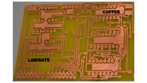
Copper plated circuit PCB
2. Importance of Copper Plating in PCB Manufacturing
Copper plating is often considered the lifeblood of PCB functionality, and nowhere is this more evident than in the role it plays within a Copper Plated Circuit PCB. As PCB designs evolve to accommodate higher speeds, denser routing, and enhanced thermal and mechanical demands, the precision and performance of copper plating have become pivotal to achieving manufacturing success.
2.1 Copper as a Conductor: Why It Matters
The most fundamental reason for using copper in PCBs is its outstanding electrical conductivity. Copper has one of the lowest resistivities among industrial metals, only second to silver. Its balance between cost-effectiveness, availability, conductivity, and workability makes it ideal for use in PCBs.
In a Copper Plated Circuit PCB, copper acts as the conduit for signal transmission and power distribution. Signals must travel rapidly and without degradation across trace routes that may span multiple layers of a complex PCB. The uniformity and quality of the copper plating on these traces directly influence signal fidelity, especially in high-speed or high-frequency designs. Inadequate plating can introduce signal attenuation, impedance mismatches, and increased electromagnetic interference (EMI).
2.2 Via Integrity and Interlayer Connectivity
Modern PCBs are multilayered structures composed of alternating layers of conductive and insulating materials. These layers must be connected vertically through holes called vias, which may be through-holes, blind vias, or buried vias.
Copper plating is used to coat the interior walls of these vias to establish reliable electrical connections between layers. The ability to form defect-free, continuous, and uniformly thick copper layers in these vias is critical to the performance of the board. Failure in the plating of these structures—such as voids, cracks, or delamination—can lead to interconnect defects (ICDs), which are major causes of board failure in the field.
In a Copper Plated Circuit PCB, these vias are often microvias or stacked vias to allow for high-density interconnects (HDI). These advanced interconnects depend even more heavily on perfect copper plating due to their minute dimensions and stringent reliability requirements.
2.3 Role in Mechanical Stability and Thermal Management
Copper not only provides electrical functionality but also contributes significantly to the mechanical integrity of the PCB. Plated copper enhances the rigidity of vias and prevents barrel cracking—a phenomenon that occurs when the PCB is exposed to thermal cycling during assembly or operation.
Additionally, copper’s excellent thermal conductivity is harnessed in power and high-frequency applications to dissipate heat effectively. Boards with heavy copper plating (e.g., 2–3 oz or more) are used in power electronics and automotive applications where thermal performance is critical.
In such scenarios, the plated copper is often extended over large surface areas or along heat-sinking paths. A Copper Plated Circuit PCB may include solid copper planes or thick copper vias that draw heat away from critical components, extending the lifespan of the electronics and enhancing system reliability.
2.4 Fine-Line Capabilities and Design Flexibility
As electronic devices become smaller and more powerful, the need for finer circuitry and tighter trace spacing becomes paramount. The copper plating process must be refined to achieve uniform copper coverage even in the narrowest trenches and microvia structures.
One of the recent breakthroughs enabling this is the modified semi-additive process (mSAP), which allows for trace widths and spaces of 15 µm or less. These ultra-fine features would not be manufacturable without highly controlled copper plating techniques.
In a Copper Plated Circuit PCB, designers rely on this capability to increase routing density, reduce layer count, and shrink the overall form factor of the device. This is particularly valuable in applications such as smartphones, wearables, and implantable medical devices where space is at a premium.
2.5 Manufacturing Yield and Cost Efficiency
From a manufacturing standpoint, consistent and defect-free copper plating has a direct impact on yield. Poorly plated boards may suffer from open circuits, delamination, or increased electrical resistance. These issues may not manifest during initial testing but can result in latent failures during field use, leading to costly product recalls or reputational damage.
In contrast, high-quality copper plating ensures that each board passes functional testing and endures real-world conditions without failure. This reliability improves production yields, reduces rework and scrap rates, and minimizes warranty claims.
Moreover, advancements in copper plating chemistry and process control allow manufacturers to plate more boards with less material waste and reduced energy consumption. For instance, pulse plating and high-efficiency electrolytic solutions enable better copper distribution in vias and trenches, using less bath time and fewer chemical inputs.
The Copper Plated Circuit PCB becomes not only a reliable product but also an economically viable one, thanks to the efficiencies gained in the copper plating step.
2.6 Influence on Signal Integrity and High-Frequency Performance
High-speed digital and RF/microwave circuits are increasingly prevalent in modern electronics. In these applications, even minor inconsistencies in copper plating can introduce signal distortion. Surface roughness, thickness variations, and edge profile irregularities all contribute to impedance mismatches and increased insertion loss.
To mitigate these issues, surface treatments such as reverse pulse plating, low-profile copper foils, and controlled grain structures are employed. These techniques result in smoother copper surfaces, which reduce signal loss and improve reflection characteristics.
In Copper Plated Circuit PCBs destined for use in 5G, automotive radar, or satellite communications, signal integrity is paramount. Manufacturers often specify precise copper thickness tolerances and grain structures to ensure predictable performance over a wide frequency range.
3. Overview of the Copper Plating Process in PCB Fabrication
In the manufacturing of a Copper Plated Circuit PCB, copper plating is not merely an auxiliary step—it is a foundational process that enables multilayer connectivity, signal transmission, and mechanical integrity. The copper plating process typically involves a series of highly controlled chemical and electrical procedures designed to deposit a consistent copper layer on both the inner hole walls and surface features of a PCB panel. Understanding this process in depth helps both engineers and quality assurance teams optimize their production yield and performance reliability.
3.1 Drilling and Desmear as Pre-Plating Prerequisites
Before copper plating can begin, the PCB panel must undergo a critical set of preparatory steps. These include drilling and desmearing, which together ensure that the internal hole walls are clean and ready for metallization.
Drilling creates the through-holes, blind vias, and buried vias needed for vertical interconnections. However, the frictional heat from drilling causes resin smear—thin layers of epoxy resin that coat the hole walls and insulate the inner copper layers from electrical contact.
Desmear involves chemically or mechanically removing this unwanted smear, typically using permanganate or plasma-based processes. The quality of desmear directly influences the ability of the copper plating to bond with the dielectric surface, especially in high-density Copper Plated Circuit PCBs where microvias are used.
3.2 Electroless Copper Deposition: Seeding the Path
Following desmear, the hole walls—now clean but non-conductive—must be seeded with a conductive layer to allow electroplating to proceed. This is done via electroless copper deposition, also known as PTH (plated through-hole) metallization.
This process relies on a chemical reaction that deposits a thin, uniform layer of copper (typically 0.5 to 1.0 µm thick) on the non-metallic surfaces. This layer acts as the foundation for subsequent electroplating.
In the context of Copper Plated Circuit PCBs, this step is crucial because it determines the electrical continuity between inner and outer layers. Voids or thin spots in the electroless copper can lead to interconnect defects (ICDs) or blowholes during soldering.
3.3 Electrolytic Copper Plating: Building Conductive Mass
With the seeding complete, the panels are immersed in an electrolytic copper plating bath where current is applied to thicken the copper layer. This process forms the main conductive paths in vias, through-holes, and surface traces.
Key elements of the electroplating process include:
-
Electrolyte Composition: A solution containing copper sulfate, sulfuric acid, and proprietary additives that influence deposit structure and leveling.
-
Current Density: Carefully controlled to achieve uniform plating thickness throughout the panel, especially in deep or narrow vias.
-
Temperature and Agitation: To enhance ion transport and prevent dendritic growth or nodular deposition.
Pulse plating, in which current is alternated at high frequencies, is increasingly used in Copper Plated Circuit PCB production. This technique improves copper distribution, enhances mechanical properties, and reduces internal stresses.
3.4 Pattern Plating for Circuit Formation
Once a uniform copper layer has been built, the board moves to the pattern plating stage, where the circuitry is defined. In this step, a photoresist is applied to mask off unwanted areas, and additional copper is plated only on the exposed areas that will form the final traces, pads, and vias.
Pattern plating requires precise control to avoid overplating, which can cause bridging between conductors, or underplating, which weakens signal traces and vias.
For Copper Plated Circuit PCBs, especially those with HDI designs, pattern plating plays a critical role in achieving the fine line widths and spaces required for high-density routing. Innovations in additive chemistry and photoresist technology have enabled trace widths of less than 25 µm while maintaining excellent adhesion and continuity.
3.5 Tin Plating and Etching
Following pattern plating, a layer of tin is electroplated on top of the copper traces to protect them during the etching process. The tin acts as an etch resist, shielding the copper underneath while the unprotected copper areas are removed.
Etching uses acid-based solutions to dissolve and remove excess copper, leaving behind only the circuit pattern defined by the tin mask. After etching, the tin is stripped away, revealing the clean copper features.
In Copper Plated Circuit PCBs, the precision of this etching process is vital. Any over-etching can lead to trace thinning or even breaks in critical connections, while under-etching may leave residual copper that could cause shorts or signal interference.
3.6 Plating Thickness and Tolerance Control
Plating thickness is a critical parameter that must be closely monitored. For most standard PCBs, finished copper thickness ranges from 1 oz/ft² (~35 µm) to 2 oz/ft² (~70 µm). However, for power electronics or thermally demanding applications, thicknesses of 3 oz/ft² or more may be required.
Advanced plating systems now use in-line thickness monitors, such as X-ray fluorescence (XRF), to measure and record copper buildup in real-time. This ensures that every Copper Plated Circuit PCB meets its specified electrical and thermal performance metrics without excessive material usage.
Too much copper can reduce trace resolution and increase cost, while too little can impair current-carrying capacity and reliability. Automated feedback systems can adjust current density and bath composition dynamically to maintain target values.
4. Process Control and Quality Assurance in Copper Plated Circuit PCB Production
In the highly precise and reliability-demanding realm of Copper Plated Circuit PCB manufacturing, maintaining stringent control over the copper plating process is not merely desirable—it is essential. The performance, durability, and electrical characteristics of PCBs are tightly bound to the consistency and integrity of copper deposition. Therefore, manufacturers must implement a robust system of process controls and quality assurance (QA) protocols that monitor, evaluate, and correct plating performance at every stage.
4.1 Monitoring Electroplating Parameters in Copper Plated Circuit PCB Fabrication
At the heart of copper plating is the electroplating bath, a complex system whose chemistry and operational parameters directly influence the quality of the deposited copper.
Key parameters include:
-
Copper ion concentration: Typically maintained between 20–50 g/L.
-
Sulfuric acid concentration: Maintained between 150–250 g/L to ensure bath conductivity.
-
Chloride ion content: Usually kept at 50–100 mg/L to influence grain structure and stress.
-
Temperature: Optimal range is 20–30°C, depending on bath additives and board design.
-
Current density: Generally between 1.5–3 A/dm², adjusted for hole size, aspect ratio, and plating thickness.
Any deviation from these target values can lead to common defects such as:
-
Void formation in vias due to poor ion transport.
-
Overplating and bridging due to excessive current density.
-
Burnt deposits due to low copper concentration or imbalance of additives.
Modern Copper Plated Circuit PCB production facilities utilize automated bath monitoring systems, often integrated with real-time feedback controls. These systems detect variations and can auto-dose required chemicals or adjust process parameters accordingly, preventing defects before they emerge.
4.2 Microsection Analysis and Metallographic Evaluation
One of the most reliable quality checks for plated-through holes and vias is the microsection test. This process involves cross-sectioning a finished PCB panel and examining it under a microscope to assess copper thickness, adhesion, uniformity, and void formation.
For Copper Plated Circuit PCBs, especially those used in high-reliability sectors like aerospace or medical devices, microsectioning is a routine requirement. The critical attributes analyzed include:
-
Plated copper thickness on the hole wall (typically ≥20 µm).
-
Uniformity of copper distribution across panel regions.
-
Adhesion and interfacial bonding to internal copper layers.
-
Presence of cracks, delamination, or voids.
Microsection results inform process adjustments and root cause analyses for any observed anomalies.
4.3 Surface Roughness and Bonding Strength Testing
Beyond internal structure, the surface characteristics of the plated copper are vital for later stages such as soldermask application, soldering, and multilayer lamination. Roughness (Ra) should be controlled to enable mechanical interlocking and surface energy optimization for coatings.
Advanced Copper Plated Circuit PCB facilities use profilometers or atomic force microscopy (AFM) to measure copper surface roughness. These readings help tune additive dosing in the bath and determine if micro-etching is needed prior to downstream steps.
In some cases, peel strength testing is used to evaluate the bond between the copper layer and substrate. This test involves pulling a copper trace off the PCB surface at a specific angle and measuring the force required. Poor adhesion values may indicate contamination, improper surface preparation, or inadequate copper grain structure.
4.4 Electroplated Via Integrity Testing
With the widespread use of microvias, blind vias, and stacked vias in Copper Plated Circuit PCB designs, ensuring via integrity becomes a priority. Poorly plated vias can cause latent failures, especially under thermal cycling or high-speed signal conditions.
Integrity tests include:
-
Time Domain Reflectometry (TDR) for electrical continuity.
-
Cross-section analysis for visual inspection of via fill.
-
Thermal shock testing to simulate field conditions.
Filled vias, especially those intended for via-in-pad designs, require tight control of plating speed and bath additives to prevent voids and ensure full densification.
4.5 Plating Line Calibration and Maintenance
Even the most advanced copper plating lines require regular calibration and maintenance to preserve precision. This includes:
-
Anode inspections to ensure uniform dissolution and avoid sludge buildup.
-
Filtration system maintenance to remove particulates and maintain electrolyte purity.
-
Cathode bar alignment to guarantee uniform current distribution across the panel.
-
Periodic dummy plating to remove excess organics and stabilize bath composition.
Some facilities adopt Statistical Process Control (SPC) methods to track long-term plating consistency and identify early warning signs of drift or deviation.
4.6 Traceability and Data Logging for Copper Plated Circuit PCB Quality
In today’s smart manufacturing environments, traceability is integral to both quality control and customer assurance. Copper plating process data—including plating time, current, bath conditions, and operator input—can be logged and associated with each batch or even each individual PCB panel.
This digital record serves multiple purposes:
-
Enables root cause analysis for any field failures.
-
Facilitates audits and certifications.
-
Supports predictive maintenance and continuous improvement.
For high-end Copper Plated Circuit PCB production, this level of data traceability is often a customer requirement and forms part of the PCB manufacturer’s competitive advantage.
5. Challenges and Solutions in High-Density Copper Plated Circuit PCB Design
As modern electronics evolve towards miniaturization and increased functionality, Copper Plated Circuit PCB designs are becoming denser and more complex. With components shrinking in size and the demand for faster signals and better thermal performance, PCB designers and manufacturers must address a host of technical and production-related challenges. The following section examines the key hurdles encountered in high-density copper-plated PCB fabrication and offers insights into how these issues are overcome.
5.1 Space Constraints and Trace Width Limitations in Copper Plated Circuit PCB
One of the most prominent challenges in high-density PCB design is the physical limitation on space. As the demand for more connections per square inch increases, the trace width and spacing must be reduced. However, when traces are too thin or placed too closely, signal integrity and manufacturing tolerances are affected.
Key issues include:
-
Trace resistance increases with thinner widths, affecting power delivery and signal loss.
-
Risk of trace bridging or shorting during copper plating or etching.
-
Difficulty in controlling etching precision with sub-3 mil traces.
Solutions:
-
Implement HDI (High-Density Interconnect) techniques such as microvias and via-in-pad to free up surface area.
-
Utilize laser direct imaging (LDI) for finer pattern definition before plating.
-
Rely on advanced dry film and liquid photoresists with high resolution to ensure narrow lines are accurately defined and maintained throughout the plating and etching steps.
5.2 Via Design and Management in Copper Plated Circuit PCB
With component density rising, traditional through-hole vias occupy too much space. High-density designs often require blind, buried, stacked, and staggered vias to preserve routing area and signal integrity. However, these via types introduce significant complexity in copper plating processes.
Challenges include:
-
Void formation in deep or high aspect ratio vias due to limited electrolyte flow.
-
Misalignment in stacked vias, which can result in weak interlayer connections.
-
Non-uniform plating thickness, especially at the knee of the via.
Solutions:
-
Introduce pulse plating or periodic reverse pulse plating, which improves throwing power and ensures uniform via wall coverage.
-
Design for manufacturability (DFM) by setting realistic aspect ratios (height to diameter of via).
-
Use via-fill plating techniques where conductive or non-conductive materials are applied before surface copper plating, improving planarization and reliability.
5.3 Thermal Management in Dense Copper Plated Circuit PCB
With increasing component density and power delivery, managing heat becomes a critical issue. Copper, with its high thermal conductivity, is both a benefit and a challenge in these scenarios. Without appropriate heat pathways or dissipation strategies, PCB layers may delaminate, and component life could be shortened.
Key problems include:
-
Hotspots near high-power ICs or RF modules.
-
Insufficient copper thickness to conduct heat away effectively.
-
Inconsistent heat sinking across different areas of the board.
Solutions:
-
Incorporate thermal vias, often copper-filled, that transfer heat from surface-mounted components to internal or bottom-layer copper pours.
-
Design copper planes or thermal pads beneath high-power devices.
-
Use embedded metal core PCBs (MCPCBs) when needed, which combine copper plating with high-conductivity substrates like aluminum or copper cores.
5.4 Signal Integrity and EMI in High-Density Copper Plated Circuit PCB
As signal frequencies increase, the physical layout of copper traces becomes a primary determinant of signal quality. Crosstalk, electromagnetic interference (EMI), and impedance mismatches can be severe in densely packed copper-plated PCBs.
Key signal integrity challenges:
-
Impedance discontinuity due to varying copper trace widths or uneven plating.
-
Cross-talk between adjacent traces, especially at higher frequencies.
-
Reflections and loss due to poor via transitions or grounding practices.
Solutions:
-
Perform impedance modeling using 3D simulation tools and adjust plating thickness accordingly.
-
Route high-speed signals on internal layers, shielded by ground planes plated with copper.
-
Use differential pairs with controlled spacing and matched length to reduce EMI and skew.
5.5 Reliability and Mechanical Stability of Copper Plated Circuit PCB
As more mechanical stress is placed on high-density PCBs (flexing during assembly, thermal cycling, etc.), the reliability of the copper plating—especially in vias—becomes a concern. Cracks in via barrels, delamination of copper layers, or plating stress-induced warping can all reduce long-term board reliability.
Issues to consider:
-
Electrochemical migration between closely spaced copper features under high humidity.
-
Crack formation in plated-through holes during reflow or thermal shock.
-
Degradation of adhesion between plated copper and dielectric materials.
Solutions:
-
Introduce post-plating annealing processes to relieve internal stress in plated copper.
-
Use low CTE (coefficient of thermal expansion) laminates, especially in multilayer boards.
-
Employ plating additives and grain refiners to control the crystal structure of deposited copper, enhancing ductility and fatigue resistance.
5.6 Manufacturing Yield and Process Capability Enhancements
As designs push the limits of manufacturability, yield losses due to plating defects, underetching, or misregistration become increasingly costly. Tight tolerances require investment in both equipment and process engineering.
Strategies to improve yield:
-
Upgrade to automated optical inspection (AOI) systems for early detection of plating defects.
-
Implement in-line bath analysis and replenishment systems to maintain plating consistency.
-
Design test coupons on every panel for in-situ verification of plating thickness, via fill, and surface finish quality.
6. Environmental and Economic Aspects of Copper Plated Circuit PCB Manufacturing
The increasing adoption of Copper Plated Circuit PCB technology across various industries, including telecommunications, automotive, aerospace, and consumer electronics, has brought about not only technical achievements but also growing scrutiny from environmental and economic perspectives. As copper plating is an energy- and chemical-intensive process, manufacturers must balance high-performance goals with environmental sustainability and cost-efficiency.
This section delves into the environmental implications of copper-plated PCB production and highlights strategies for minimizing environmental impact while optimizing economic outcomes.
6.1 Resource Consumption in Copper Plated Circuit PCB Production
One of the most significant environmental impacts of copper-plated PCB manufacturing is the high consumption of resources. These include:
-
Raw copper: Used for electroplating and base laminates.
-
Electricity: Required for the electroplating process, heating, and automated systems.
-
Water: Extensively used for rinsing between chemical baths, cleaning residues, and cooling.
-
Chemicals: Acids, alkalis, additives, surfactants, and stabilizers are needed in large quantities.
Particularly in large-scale operations, the energy consumed for copper electroplating is considerable, sometimes accounting for more than 30% of a facility’s total electrical usage.
Environmental mitigation strategies:
-
Install closed-loop water recycling systems to reduce freshwater usage.
-
Use pulse-reverse plating to increase efficiency and reduce overuse of chemicals.
-
Source recycled copper or copper alloys when possible, lowering dependence on virgin mining.
6.2 Wastewater and Sludge Management in Copper Plated Circuit PCB
The copper electroplating process generates a considerable amount of wastewater laden with heavy metals, complexing agents, and suspended solids. Improper disposal of this wastewater leads to soil and groundwater contamination, posing a risk to both ecosystems and human health.
Additionally, plating sludge—a byproduct rich in copper hydroxide and other residues—is categorized as hazardous waste and must be treated accordingly.
Solutions and best practices:
-
Utilize ion-exchange columns and membrane filtration to recover copper from rinse water.
-
Implement precipitation-neutralization techniques to convert soluble copper into solid forms for safe disposal.
-
Invest in sludge dewatering and metal recovery systems that convert waste into reusable metal products.
Governments and environmental agencies have placed stricter regulations on the disposal of metal-bearing effluents, compelling manufacturers to embrace more sustainable waste management practices.
6.3 Air Emissions and Occupational Safety in Copper Plated Circuit PCB Facilities
Though copper electroplating is a mostly liquid-phase process, some air emissions still occur, especially in facilities that lack proper ventilation or fume scrubbing systems. These include:
-
Hydrogen gas released during plating.
-
Acid mists containing sulfuric or hydrochloric acid.
-
Volatile Organic Compounds (VOCs) from auxiliary treatments.
Operators exposed to prolonged concentrations of fumes may experience health effects, including respiratory irritation and dermatitis. Therefore, ensuring a safe working environment is paramount.
Protective measures:
-
Use acid mist suppressants and hooded plating lines to capture emissions at the source.
-
Maintain active fume extraction and scrubbing units.
-
Train staff in chemical handling protocols and provide PPE (personal protective equipment) consistently.
In addition to regulatory compliance, workplace safety initiatives foster employee retention and improve operational reputation.
6.4 Economic Costs of Copper Plated Circuit PCB Manufacturing
From a business perspective, copper-plated PCBs offer high reliability and performance, but they also come with notable cost factors:
-
Capital investment in plating equipment, filtration systems, automation, and cleanroom facilities.
-
Operational expenses due to electricity, labor, maintenance, and raw material prices.
-
Yield loss and rework in the event of plating defects, especially in complex multilayer or HDI boards.
-
Environmental compliance costs, including permits, monitoring, and third-party audits.
Despite these expenses, copper-plated PCBs remain cost-effective over the product lifecycle, particularly when considering their role in enabling miniaturization, high-speed data transfer, and thermal performance.
Cost optimization strategies:
-
Adopt lean manufacturing principles to eliminate waste and streamline workflows.
-
Use real-time monitoring systems for bath chemistry and plating parameters to avoid defects.
-
Consolidate multi-process stations to reduce handling and downtime.
6.5 Transitioning to Green Chemistry in Copper Plated Circuit PCB Production
To address both economic and environmental demands, many manufacturers are transitioning toward green chemistry approaches in copper plating. This involves replacing toxic substances with benign alternatives and designing processes that reduce waste at the source.
Examples include:
-
Switching from cyanide-based to non-cyanide copper solutions.
-
Replacing traditional surfactants with biodegradable wetting agents.
-
Using electrochemical recovery units that recycle copper ions in real time.
These initiatives not only minimize ecological impact but also reduce long-term operating costs, as fewer chemicals are wasted and less remediation is required.
6.6 Sustainable Supply Chain and End-of-Life Considerations
Another often-overlooked aspect of environmental and economic impact is the supply chain footprint and the fate of PCBs at the end of their lifecycle.
Concerns include:
-
Mining impacts associated with virgin copper extraction.
-
E-waste management, where improperly disposed PCBs contribute to toxic landfill build-up.
-
Product take-back and recycling complexity, especially for boards with mixed-metal layers and laminated construction.
Improvement opportunities:
-
Partner with suppliers committed to sustainable mining and ethical sourcing.
-
Design boards for disassembly and metal recovery, such as using modular PCBs.
-
Invest in or collaborate with PCB recycling infrastructure capable of extracting copper, gold, and other valuable materials from end-of-life products.
7. Quality Assurance and Testing Protocols for Copper Plated Circuit PCB
The performance and reliability of Copper Plated Circuit PCB assemblies are deeply dependent on the precision of the copper plating process. A minor deviation in plating thickness, adhesion, or conductivity can lead to serious electrical failures, corrosion, or reduced product lifespan. Therefore, a robust framework for quality assurance and testing is essential.
This section explores key protocols, testing methods, and inspection technologies used to maintain consistent quality in copper-plated PCBs throughout the manufacturing cycle.
7.1 Importance of Testing in Copper Plated Circuit PCB Fabrication
Copper plating serves as the backbone for conducting signals, distributing power, and enabling interlayer connections. Any flaw in this layer compromises the functionality of the entire board. Thus, manufacturers employ rigorous testing at multiple stages:
-
Before plating (substrate cleanliness and hole preparation),
-
During plating (bath condition monitoring, real-time thickness),
-
After plating (adhesion, integrity, conductivity tests).
The goal is to detect and eliminate anomalies before they propagate downstream in the production line or reach the end-user.
7.2 Visual Inspection and Automated Optical Inspection (AOI) in Copper Plated Circuit PCB
The initial layer of quality control often involves visual inspection, where trained technicians check for obvious defects such as:
-
Blistering or peeling copper,
-
Uneven surface finish,
-
Exposed base material,
-
Voids around vias or pads.
However, given the limitations of manual observation, Automated Optical Inspection (AOI) systems are employed for greater speed and precision. These systems use high-resolution cameras and pattern recognition algorithms to scan and compare copper patterns against design files (Gerber data).
AOI is effective for detecting:
-
Misregistration of plating,
-
Over-etching or under-etching,
-
Breaks or shorts in copper traces.
7.3 Cross-Section Analysis in Copper Plated Circuit PCB Evaluation
To assess internal copper plating conditions—especially in vias, microvias, and through-holes—manufacturers perform cross-section analysis.
This process involves:
-
Cutting a sample PCB vertically across a plated feature,
-
Mounting and polishing the cross-section,
-
Observing under a microscope.
Parameters evaluated include:
-
Copper wall thickness in plated through-holes (PTH),
-
Uniformity of plating coverage,
-
Void or delamination between plating and dielectric.
Cross-sectioning is a destructive test but offers invaluable insight into plating conformity and structural reliability.
7.4 Microsection Testing and IPC Class Standards
Microsection testing goes beyond visual inspection by analyzing minute structural features under high magnification. The method complies with IPC-A-600 and IPC-6012 standards, which define acceptability criteria for plated PCBs.
Microsection tests evaluate:
-
Minimum and maximum plating thickness,
-
Copper nodule formation and uniformity,
-
Adhesion between copper and the substrate,
-
Evidence of corrosion, cracks, or inclusions.
Manufacturers often categorize boards into IPC Class 1, 2, or 3, depending on the application:
-
Class 1: General electronic products,
-
Class 2: Dedicated service electronics (long life, uninterrupted service),
-
Class 3: High-reliability applications (medical, aerospace, military).
Copper plating standards are most stringent for Class 3.
7.5 Conductivity and Continuity Testing in Copper Plated Circuit PCB
Electrical functionality is the ultimate test of success for copper plating. Therefore, conductivity and continuity tests are indispensable.
Four-point probe method:
-
Measures sheet resistance of copper layers,
-
Ensures consistent conductivity across the surface.
Flying probe and bed-of-nails testers:
-
Inject signals into test points,
-
Confirm that current flows across all designated traces and connections,
-
Identify open circuits or short circuits.
Many manufacturers employ automated testing systems that run hundreds or thousands of probes simultaneously, drastically reducing time for high-volume orders.
7.6 Peel Strength and Adhesion Testing in Copper Plated Circuit PCB
The adhesion between plated copper and the substrate must be strong enough to withstand thermal cycling, mechanical vibration, and cleaning processes. One method to measure this is peel strength testing.
Procedure:
-
A narrow strip of plated copper is etched and pulled away from the substrate at a defined angle.
-
The force required is recorded in pounds/inch or Newtons/meter.
Factors influencing adhesion include:
-
Surface roughness of the laminate (promotes mechanical anchoring),
-
Pre-plating cleaning quality,
-
Presence of oxide layers or contaminants.
Failing peel strength tests can lead to product recalls, especially in mission-critical applications.
7.7 Reliability Testing for Copper Plated Circuit PCB Under Stress Conditions
In addition to in-line testing, long-term reliability tests simulate real-world environmental conditions to evaluate how copper plating will perform over time. These include:
-
Thermal shock and cycling: Repeated heating and cooling to detect delamination or crack propagation.
-
Humidity testing: Evaluates corrosion resistance in high-moisture environments.
-
Salt spray testing: For boards exposed to marine or automotive environments.
-
Vibration and mechanical fatigue: Important for aerospace and automotive boards.
Data from these tests feed into failure mode and effect analysis (FMEA) systems that help refine design and manufacturing parameters.
7.8 Inline Monitoring and Smart QA in Copper Plated Circuit PCB Manufacturing
Modern PCB manufacturers increasingly rely on smart QA systems, integrating data analytics and machine learning to improve defect detection and prediction.
Real-time monitoring tools track:
-
Plating current density,
-
Bath chemistry (copper ion concentration, pH, temperature),
-
Surface thickness using laser profilometers or X-ray fluorescence (XRF).
Automated alerts can stop production lines or adjust process parameters before defects occur, saving costs and reducing waste.
Cloud-based dashboards allow quality managers to view data across multiple factories, track KPIs, and ensure compliance with internal or customer-specific standards.
8. Applications and Future Trends in Copper Plated Circuit PCB Technology
As electronics continue to evolve across industries—be it automotive, telecommunications, healthcare, or aerospace—the role of Copper Plated Circuit PCB has become more foundational than ever. The copper plating process is not just a legacy necessity; it’s a dynamic technology constantly adapting to meet emerging challenges in performance, miniaturization, and durability.
This section explores key application areas where copper-plated PCBs shine and evaluates the technological trends shaping their future.
8.1 Copper Plated Circuit PCB in High-Speed Digital Devices
One of the foremost uses of Copper Plated Circuit PCB is in high-speed digital devices such as computers, servers, routers, and cloud infrastructure systems. As data transfer rates increase into gigahertz and even terahertz frequencies, maintaining signal integrity becomes a top priority.
Copper plating contributes significantly to:
-
Low impedance signal transmission through plated vias and planes,
-
Thermal management, dissipating heat from densely packed ICs,
-
Reliability, especially under constant power cycling and electromagnetic interference.
Applications include:
-
High-performance computing (HPC),
-
AI accelerator boards (GPU/TPU clusters),
-
Advanced driver-assistance systems (ADAS) for vehicles.
8.2 Copper Plated Circuit PCB in Electric Vehicles and Power Electronics
The global push toward electrification of transportation is driving new demand for robust and high-current PCBs. Copper Plated Circuit PCB provides the ideal platform for these applications due to its excellent conductivity and high current-carrying capacity.
In EVs, such PCBs are used in:
-
Battery management systems (BMS),
-
Inverters and motor controllers,
-
On-board chargers (OBCs),
-
Power distribution units (PDUs).
To support these functions, manufacturers are developing heavy copper PCBs with plating thicknesses up to 12 oz/ft². These designs improve:
-
Short-circuit resistance,
-
Thermal cycling endurance,
-
Mechanical durability under high torque and vibration.
8.3 Copper Plated Circuit PCB in 5G and RF Applications
5G communication systems demand ultra-low latency and extremely high bandwidth. This requires PCBs with tight impedance control, low signal loss, and superior surface smoothness. Copper-plated PCBs rise to this challenge with high-density interconnect (HDI) layouts and fine-line features.
Notable features in this context include:
-
Microvia copper plating to create stacked vias for multilayer RF modules,
-
Smooth copper finish to minimize insertion loss at millimeter-wave frequencies,
-
Hybrid laminates with plated interconnects, combining rigid and flexible substrates.
Use cases include:
-
5G base stations,
-
mmWave antenna modules,
-
Smart home routers and gateways.
8.4 Copper Plated Circuit PCB in Medical and Wearable Technology
Medical electronics place high demands on miniaturization, biocompatibility, and long-term reliability. Copper Plated Circuit PCB meets these needs through precision plating and high-density interconnect technologies.
Applications include:
-
Implantable devices (e.g., pacemakers),
-
Diagnostic equipment (e.g., MRI, CT scanners),
-
Wearable health monitors and biosensors.
In wearable tech, flex-rigid PCB formats with plated copper layers allow:
-
Lightweight and low-profile designs,
-
Enhanced signal integrity even during movement,
-
Power routing across flexing components.
8.5 Copper Plated Circuit PCB in Aerospace and Military Applications
Aerospace and defense sectors demand the highest level of reliability, often under extreme temperature fluctuations, radiation exposure, and mechanical stress. Copper-plated PCBs are engineered to meet these demands.
Technologies employed include:
-
Via-in-pad plating for compact and reliable BGA connections,
-
Multilayer copper redistribution, offering EMI shielding and controlled impedance,
-
Advanced reliability testing, such as HALT/HASS (Highly Accelerated Life Testing/Stress Screening).
Use cases involve:
-
Avionics systems,
-
Radar modules,
-
Satellite electronics,
-
Navigation and guidance systems.
8.6 Environmental Impact and Sustainable Approaches in Copper Plated Circuit PCB Production
As PCB demand increases, so does the environmental burden of chemical processing, particularly during copper electroplating. Sustainability is becoming a focal point in future development.
Green manufacturing initiatives include:
-
Closed-loop electrolyte recycling systems, reducing heavy metal discharge,
-
Low-temperature plating to reduce energy usage,
-
Environmentally friendly etchants and rinsing agents,
-
Life cycle analysis (LCA) to track and reduce environmental impact.
Manufacturers are also exploring direct metallization and additive processes to replace or supplement conventional copper plating with more eco-conscious techniques.
8.7 The Future of Copper Plated Circuit PCB: Trends and Innovations
Looking ahead, several trends are set to redefine the landscape for Copper Plated Circuit PCB technology:
-
Nano-copper plating: Enhanced surface area and thermal/electrical performance,
-
Pulse reverse plating: Better surface uniformity and via fill performance,
-
Automated quality prediction using AI and machine learning,
-
Additive manufacturing (AM) of copper features via inkjet or laser printing,
-
Integration with advanced packaging like system-in-package (SiP) and 2.5D/3D ICs.
In addition, tighter design tolerances and materials innovation will require the copper plating process to adapt in terms of both selectivity and scalability.
8.8 Cross-Industry Collaboration and Standardization for Copper Plated Circuit PCB
As global demand for high-reliability PCBs rises, especially in mission-critical applications, industry stakeholders must work together to set unified benchmarks.
Efforts include:
-
Aligning with IPC and IEC standards,
-
Joint R&D ventures between OEMs, PCB fabs, and plating chemical suppliers,
-
Adoption of digital thread frameworks to ensure traceability and compliance from raw copper to finished product.
Standardization will not only improve interoperability but also reduce time-to-market and enhance global competitiveness.
9. Challenges and Solutions in Copper Plated Circuit PCB Manufacturing
While Copper Plated Circuit PCB technology has enabled transformative advancements across many electronic domains, its manufacturing processes are fraught with a range of technical, chemical, and operational challenges. These challenges affect cost, product reliability, production scalability, and environmental compliance. In this section, we explore these critical issues and provide an in-depth look at the innovative solutions that industry stakeholders are implementing to ensure continuous improvement.
9.1 Surface Preparation Challenges in Copper Plated Circuit PCB
One of the earliest and most crucial steps in copper plating is proper surface preparation. Poor surface conditions—such as residual oxide films, organic contaminants, or improper micro-etching—can result in poor copper adhesion and plating defects.
Common issues:
-
Incomplete removal of drilling residues and debris,
-
Oxidation of base copper before plating,
-
Over-etching or under-etching.
Solutions:
-
Optimized desmear processes using permanganate or plasma cleaning,
-
Micro-etch control systems that monitor surface roughness in real-time,
-
Advanced scrubber designs with uniform brush pressure and automated height adjustment.
Implementing inline surface analytics, such as contact angle measurement and reflectivity testing, further enhances surface quality assurance.
9.2 Uniformity and Thickness Control in Copper Plated Circuit PCB
Achieving uniform copper thickness across a PCB—especially in high-aspect-ratio through-holes and blind vias—is a central challenge in the copper plating process. Non-uniform plating can lead to:
-
Open circuits or excessive resistance in thin areas,
-
Short circuits or clearance violations in over-plated areas,
-
Voids or fractures during reflow or stress testing.
Solutions:
-
Pulse plating and pulse reverse plating techniques, which allow better electrolyte penetration into vias and cavities,
-
Robotic agitation systems that provide controlled electrolyte flow and turbulence across the board surface,
-
Cathode bar optimization to balance current density distribution.
These methods ensure better plating uniformity and improve the overall mechanical strength of interconnects.
9.3 Copper Waste Management in Copper Plated Circuit PCB
Copper electroplating generates a significant amount of waste, including spent electrolytes, copper-laden rinse water, and sludge. Without proper disposal or recycling, this waste poses serious environmental hazards and regulatory challenges.
Key concerns:
-
Heavy metal discharge into waterways,
-
High chemical consumption,
-
Elevated operating costs from waste treatment.
Solutions:
-
Closed-loop electrolyte recovery systems using membrane filtration and ion-exchange technology,
-
Regenerative rinsing systems that drastically reduce water usage,
-
Automated sludge drying and metal reclamation units to recover copper from waste streams.
Sustainability-focused PCB manufacturers are adopting ISO 14001-compliant systems and working with environmental agencies to ensure compliance.
9.4 Microvia Plating and Filling in Copper Plated Circuit PCB
As PCBs become more compact and layered, the use of microvias—often stacked or staggered—has become standard. Plating and filling these microvias reliably is technically challenging, especially in HDI (High-Density Interconnect) boards.
Common problems:
-
Incomplete via fill (creating voids),
-
Voiding or copper pullback under thermal cycling,
-
Uneven surface leveling affecting subsequent layers.
Solutions:
-
Copper via fill additives that promote conformal and void-free plating,
-
Advanced DC and pulse-reverse rectifiers designed specifically for HDI applications,
-
Via-filling simulation software to optimize plating parameters based on via size and board design.
Companies also use X-ray and SEM (Scanning Electron Microscopy) for microvia inspection, enabling early detection of voids and irregularities.
9.5 Adhesion and Delamination Issues in Copper Plated Circuit PCB
Delamination between plated copper and dielectric material is a critical failure mode, often exacerbated during thermal stress testing or solder reflow processes.
Root causes:
-
Inadequate surface roughening prior to plating,
-
Thermal mismatch between layers,
-
Contamination or poor lamination processes.
Solutions:
-
Use of oxide replacement adhesion promoters that are compatible with lead-free and high-temperature reflow,
-
Introduction of laser roughening techniques to selectively treat surfaces at micron-scale resolution,
-
Integration of automated peel strength testing during final inspection.
Improving adhesion is especially vital for flex-rigid and high-layer-count PCBs used in aerospace and automotive applications.
9.6 Process Traceability and Quality Control in Copper Plated Circuit PCB
In high-reliability industries, traceability and documentation are as important as product performance. Tracking each step of the copper plating process is essential for root cause analysis and continuous quality improvement.
Quality control challenges:
-
Data silos between plating and inspection departments,
-
Inconsistent measurement of plating thickness and via quality,
-
Delays in failure analysis.
Solutions:
-
MES (Manufacturing Execution System) integration to log all process parameters in real time,
-
In-situ copper thickness gauges (e.g., XRF—X-ray Fluorescence),
-
Use of digital twin technology to simulate and optimize copper flow and temperature distribution in electroplating tanks.
Standardized checklists and quality gates ensure that no board advances without fulfilling all plating quality criteria.
9.7 Scaling Production of Copper Plated Circuit PCB for Mass Customization
In today’s market, PCB manufacturers must offer high-volume output while accommodating customized board layouts, thicknesses, and via configurations. This complexity makes scaling copper plating operations more demanding.
Production constraints:
-
Equipment bottlenecks due to long cycle times,
-
Recipe management complexity for varied board designs,
-
Human error in parameter selection and setup.
Solutions:
-
Automated plating lines with programmable tank sequences and recipe management,
-
Use of AGVs (Automated Guided Vehicles) and robotic handlers to streamline board movement,
-
Real-time performance dashboards for predictive maintenance and capacity optimization.
AI-based process tuning is also being adopted to autonomously adjust copper thickness based on in-line sensor feedback.
9.8 Enhancing Reliability Standards in Copper Plated Circuit PCB
As PCBs are deployed in life-critical applications, expectations for long-term reliability are rising. Copper plating must endure tens of thousands of thermal cycles, mechanical stress, and exposure to moisture, chemicals, and radiation.
Reliability challenges:
-
Copper migration and dendritic growth in humid conditions,
-
Electromigration leading to shorts under bias,
-
Cracking of plated through-holes over time.
Solutions:
-
Nano-barrier coatings post-plating to prevent moisture ingress,
-
Advanced thermal cycling and HAST testing (Highly Accelerated Stress Testing),
-
Embedded monitoring structures (e.g., daisy chains) for real-time failure tracking.
Developing fail-safe PCBs through better copper metallurgy, controlled plating chemistries, and robust testing regimes is central to future-proof designs.
10. Conclusion and Industry Outlook on Copper Plated Circuit PCB
10.1 Summarizing the Essence of Copper Plated Circuit PCB
Over the course of this detailed exploration, we have traced the evolution, methodologies, challenges, and innovations associated with Copper Plated Circuit PCB technologies. From the foundation of substrate preparation and drilling, through the intricate steps of chemical surface treatment, plating, inspection, and testing, to the final reliability assurance, copper plating stands as both a cornerstone and a gateway in printed circuit board fabrication.
The application of copper plating is not merely about depositing metal onto a surface—it is a highly controlled metallurgical and chemical engineering process that defines the electrical, thermal, and mechanical integrity of modern electronic systems. Copper not only ensures superior conductivity but also reinforces interconnect reliability across multi-layer boards, particularly in high-density and high-speed designs.
Throughout the PCB industry, the pursuit of consistent copper quality has driven manufacturers to innovate and integrate systems that deliver unmatched precision. These solutions range from pulse-reverse plating to predictive process control, from chemical analytics to automated defect mapping, and from environmental recovery to AI-driven recipe tuning. Together, these tools empower manufacturers to exceed the stringent demands of next-generation electronics.
10.2 Industry-Wide Impact of Copper Plated Circuit PCB
The implications of refined copper plating methods extend far beyond the fabrication floor. For OEMs (Original Equipment Manufacturers), contract manufacturers, and end-users, the copper quality on a PCB represents trust in performance and durability. Whether it’s a data center handling terabytes of traffic, a military drone in high-altitude turbulence, or a medical device administering life-saving pulses, all these systems depend heavily on the resilience of copper interconnects.
Moreover, the adaptation of advanced Copper Plated Circuit PCB methods has catalyzed massive shifts in design capabilities. Engineers are now able to:
-
Route signals through microvias with improved signal integrity,
-
Integrate embedded passives within inner copper layers,
-
Minimize power losses even at GHz-level signal frequencies,
-
Enhance thermal conductivity for high-power electronics.
As a result, copper plating no longer serves just as a fabrication necessity but as a design enabler and a competitive differentiator across industries such as 5G, autonomous vehicles, satellite systems, IoT, and edge computing.
10.3 Sustainability and Copper Usage Trends in PCB Manufacturing
As the industry continues to evolve, the sustainability aspect of copper usage becomes increasingly significant. While copper is a widely available resource, its large-scale mining and industrial use contribute to environmental degradation if not managed properly. The growing focus on eco-conscious manufacturing has prompted PCB manufacturers to re-evaluate copper lifecycle management.
Emerging approaches include:
-
Circular manufacturing, where copper scrap from plating tanks is recycled directly back into feedstock,
-
Green chemistries, replacing traditional acidic solutions with biodegradable or low-toxicity counterparts,
-
Energy-efficient electroplating systems, reducing power consumption per board.
Manufacturers certified under ISO 14001 or participating in initiatives like Green Electronics Council’s EPEAT are leading the way toward a more sustainable electronics supply chain, in which copper usage is optimized and environmental impact is minimized.
10.4 Future Outlook for Copper Plated Circuit PCB Technology
The future of Copper Plated Circuit PCB is undeniably promising and filled with technological evolution. Several trends and innovations are poised to reshape the way copper plating is approached in the coming years:
A. Additive Manufacturing and 3D Plating
With the rise of 3D printing in electronics, additive copper deposition is gaining traction. Instead of subtractive etching and extensive chemical baths, future PCB builds may employ precision-directed electroplating in selected areas, drastically reducing waste and production times.
B. Hybrid Materials and Conductive Inks
As alternative materials (such as graphene, carbon nanotubes, and silver nanoparticle inks) enter the scene, copper plating will need to interface seamlessly with these substrates. New adhesion promoters and interlayer connectors are under research to support hybrid circuits.
C. Artificial Intelligence in Plating Process Control
AI models trained on historical plating data, real-time sensor feedback, and defect images are beginning to predict process drift, adjust chemistries autonomously, and optimize current density distributions to an unprecedented degree.
D. Advanced Reliability Standards for Aerospace and Defense
Defense contractors and aerospace OEMs are driving demand for zero-defect copper plating. The new generation of IPC standards (e.g., IPC-2221B and IPC-6012E) reflects this shift, requiring higher peel strength, corrosion resistance, and dielectric withstanding capabilities for plated copper.
E. Miniaturization Meets Robustness
As boards shrink but function grows, high-aspect-ratio vias and ultra-thin lines are becoming standard. Precision copper plating must evolve to support geometries that push the limits of physics while maintaining fault-free conductivity and endurance.
10.5 The Strategic Role of Copper Plated Circuit PCB in the Electronics Ecosystem
It is not an overstatement to say that copper plating is the strategic link between PCB fabrication and electronic system performance. The reliability of a solder joint, the latency of a signal, the dissipation of heat, and the impedance of a trace—all hinge upon the fidelity of copper deposition.
By mastering this technology, manufacturers unlock several strategic advantages:
-
Yield improvement through fewer plating defects,
-
Scalability across prototypes to millions of units,
-
Compliance with international environmental and reliability standards,
-
Differentiation in high-speed and high-density board markets.
Therefore, investment in Copper Plated Circuit PCB process refinement is not just a tactical improvement but a strategic imperative for any forward-looking PCB or electronics manufacturing enterprise.
10.6 Final Thoughts
In conclusion, Copper Plated Circuit PCB technologies represent a refined blend of science, engineering, and craftsmanship. They bridge the worlds of materials science, electrochemistry, manufacturing automation, and electronic design. With the continued push toward smarter, faster, lighter, and more energy-efficient devices, the role of copper—and by extension, copper plating—will become even more central to the future of innovation.
As industries grow more interconnected and digital systems become omnipresent, the silent yet critical infrastructure of copper-plated interconnects will keep the heart of electronics beating reliably and efficiently.
Manufacturers, engineers, and designers who understand the nuances of copper plating will not only ensure product excellence but will lead the next chapter of electronic transformation—one micron-thick layer of copper at a time.

- long board pcb
- Flexible PCBs
- Special PCB
- Express Printed Circuit Board
- Pcb Prototype
- LED PCB
- PCB
- Printed Circuit Board
- Pcb meaning
- Pcb manufacturer
- Rigid pcb board
- Rigid Flex PCB
 Quote
Quote
 E-mail