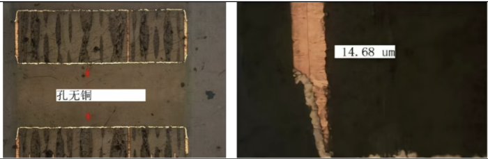
The presence of copper-free holes in printed circuit boards (PCBs) can be a significant issue that affects the quality and functionality of the final product. Copper-free holes are typically found in the drilled hole areas where copper plating fails to coat the inner surface properly. This issue can occur at various stages of PCB manufacturing, from drilling to copper plating and surface treatments. Below is an analysis of the common causes of copper-free holes in PCBs, along with explanations and solutions for each stage.
1. Drilling Process
The drilling process is a critical step in PCB manufacturing, and several issues during drilling can result in copper-free holes:
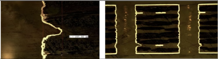
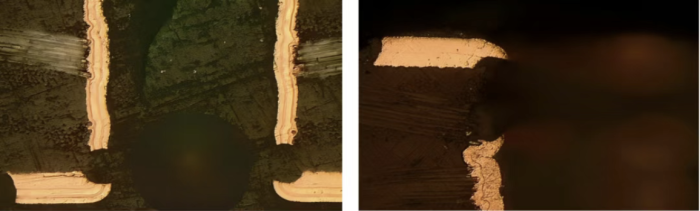
- Excessive Drill Roughness: Large roughness in the drilled hole can lead to copper plating failure. According to IPC standards, for double-sided boards, the drill roughness should be within 30 microns, and for multilayer boards, it should be no more than 25.4 microns. If the roughness exceeds these values, it may hinder the copper plating process, causing the holes to remain copper-free.
Analysis of Copper-Free Holes
- Drill Burrs: Drill burrs can cause the hole diameter to become smaller or obstructed, leading to blocked holes and poor plating results. In some cases, burrs can also lead to the formation of holes that are partially or completely blocked during the acid etching process, preventing copper from plating properly.
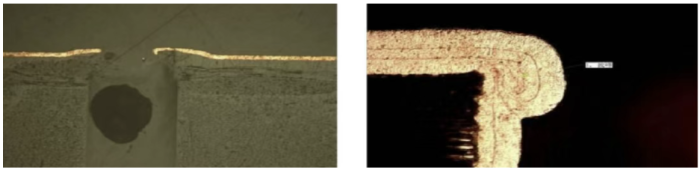
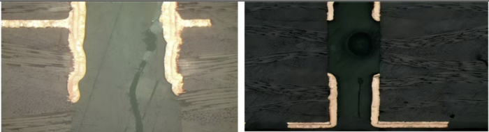
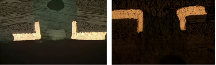
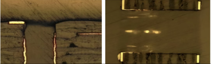
- Broken Drill Bits: Broken drill bits can cause the drilling process to fail completely, resulting in copper-free holes. This is often a mechanical failure that interrupts the drilling of the holes.
Broken Drill Bits
- Dust Blockage: During the drilling process, dust accumulation, especially at the hole exit positions, can obstruct the hole, preventing copper from properly plating inside. This is particularly common in larger or more complex hole arrangements.
Dust Blockage
-
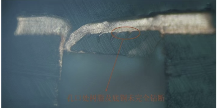
Uncut Resin and Bottom Copper
Uncut Resin and Bottom Copper: In some cases, the resin or bottom copper layer is not fully cut during the drilling process, which can result in improper copper plating on the hole walls.
2. Copper Plating Process
After drilling, the PCB undergoes copper plating, a process that coats the hole walls with a layer of copper. Several factors can lead to copper-free holes during plating:
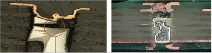
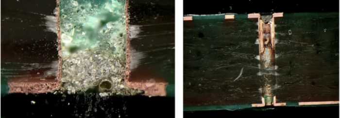
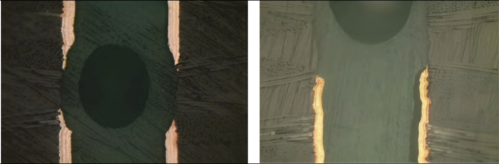
- Gas Bubble-Type Copper-Free Holes: These are characterized by holes where the copper is missing in the center, and the breakdown occurs symmetrically. The copper layer on the surface of the PCB remains intact, but the copper plating does not cover the inner walls of the hole.
Gas Bubble-Type Copper-Free Holes
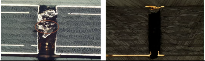
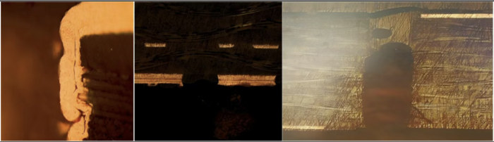
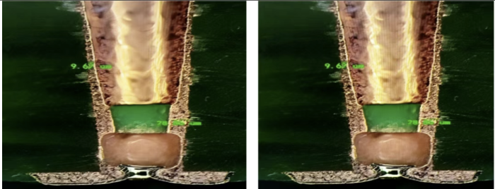
- Backlight Defects in Copper Plating: These copper-free holes occur due to poor copper deposition inside the hole. The fiberglass at the hole’s inner surface is often broken, causing intermittent copper deposition. As a result, the hole may have spotty copper deposition.
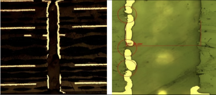
Backlight Defects in Copper Plating
- No Copper Electroplating: In some cases, only a thin copper layer is deposited on the surface, and the inner hole remains copper-free. This is typically caused by insufficient copper plating in the hole during the electroplating process.
3. Outer Layer Pattern Formation
The formation of the outer layer pattern, which involves copper etching and coating, is another crucial step where copper-free holes can occur:
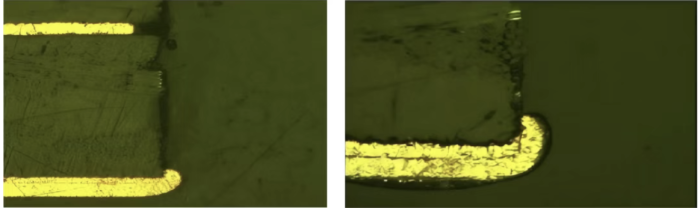
- Copper Breakage at the Hole Edge: In some instances, copper can break off at the edge of the hole, leaving the inner surface copper-free. The breakage is typically clean and occurs when the dry film resist enters the hole during the etching process.
- Dry Film Blockage: Blockage of the hole due to dry film resist, which prevents copper plating, is a common issue. The resist film can clog the hole, resulting in copper-free spots.
- Volcanic Ash Blockage in Line Pre-Treatment: The blockage caused by volcanic ash during line pre-treatment can also contribute to copper-free holes. This often occurs when the PCB is not thoroughly cleaned before plating.
- Incomplete Development of Outer Layer Circuitry: If the outer layer’s circuitry is not fully developed during the etching process, it can cause irregularities in copper plating, leading to copper-free holes. This typically happens when the ring holes or the areas between the graphic copper layer and the full board copper layer are eroded or contain debris.
- Defects in Negative Image Board: Negative image defects, such as poor exposure or scratched dry film, can cause copper-free holes. These defects are often more prominent in larger holes, especially when the second full-board electroplating does not cover the initial electroplating.
4. Electroplating Process
Electroplating is another stage where copper-free holes can occur, particularly when plating with solder:
- Bubble Type Solder Plating Defects: These types of copper-free holes are typically located in the center of the hole, with a sloped edge at the break point. These defects mostly appear in smaller holes and occur due to the inability of the electroplating process to fully deposit copper inside the hole.
5. Solder Mask
Solder mask is essential for protecting the copper traces on the PCB. However, improper application can also lead to copper-free holes:
- Ink Blockage: Ink blockage can cause copper to be removed or eroded inside the hole. This is often due to residual etching solution within the holes that affects the copper plating during the solder mask application.
6. Surface Treatment
In surface treatment processes such as nickel-gold plating, OSP, or hot air solder leveling (HASL), copper-free holes can occur due to over-etching or poor treatment:
- Over-Etching During Surface Treatment: Over-etching or excessive treatment in processes such as nickel-gold or tin-plating can lead to a complete lack of copper in both small and large holes. This typically happens when the plating solution penetrates the hole excessively, eroding the copper or causing it to be insufficiently plated.
- Uneven Copper Plating: During the surface treatment, the copper layer may become thin or uneven, especially in larger holes. This happens when the micro-etching process is not carefully controlled, resulting in insufficient copper thickness or complete copper removal.
Conclusion
Copper-free holes in PCBs can be caused by multiple issues during the manufacturing process. These issues can occur during drilling, copper plating, pattern formation, and surface treatment stages. To prevent these defects, careful attention must be given to each step, including proper drilling techniques, effective plating methods, and precise treatment processes. By addressing these common causes and implementing quality control measures, PCB suppliers can improve the quality and reliability of PCBs.
SQPCB, known for its high-quality PCBs, employs strict quality control measures to address these challenges and produce reliable products that meet the highest industry standards.

- long board pcb
- Flexible PCBs
- Special PCB
- Express Printed Circuit Board
- Pcb Prototype
- LED PCB
- PCB
- Printed Circuit Board
- Pcb meaning
- Pcb manufacturer
- Rigid pcb board
- Rigid Flex PCB
 Quote
Quote
 E-mail