1. Introduction
In the ever-evolving landscape of electronic design, one of the most critical areas of innovation lies beneath the surface—literally. As electronic devices become more powerful, compact, and thermally demanding, the printed circuit board (PCB) has evolved far beyond its original purpose of simple electrical interconnection. Today, PCBs serve as complex mechanical and thermal management systems, capable of influencing a product’s performance, reliability, and lifespan. Among the many technological advancements contributing to this evolution, a particularly compelling innovation has emerged: the integration of copper coins into PCBs.
Copper Coin PCBs represent a nuanced solution to a problem that has grown increasingly urgent—how to dissipate the ever-rising levels of heat generated by high-power components. While passive and active cooling systems such as heatsinks, fans, and even liquid cooling have been employed across various industries, there is a growing recognition that heat must be addressed not just externally, but internally—from within the PCB itself. This is where the use of embedded copper coins becomes not just relevant, but transformative.
Unlike traditional PCBs that rely solely on vias and copper planes to transfer heat, copper coins are solid inserts of high-conductivity copper strategically placed beneath power-dense components. This approach offers a direct, efficient thermal path from the component to the heat sink or chassis, significantly reducing thermal resistance and enhancing overall thermal performance. But the advantages of this technique extend far beyond heat management.
This article explores the many pros of using copper coins in PCB design from a holistic perspective. From electrical conductivity and mechanical robustness to miniaturization and integration with emerging technologies, copper coin solutions offer a multi-dimensional benefit package that is reshaping how engineers and product designers approach high-performance systems.
From my perspective as someone who has spent years analyzing, discussing, and implementing thermal management strategies in high-reliability electronics, the shift toward embedded copper coins reflects a broader trend toward system-level thinking. No longer can we treat heat as a byproduct to be managed after the fact. Instead, modern design philosophies demand that thermal performance be embedded into the very fabric of the electronics—from the silicon to the substrate. Copper Coin PCBs embody this philosophy, serving as a bridge between electrical function, mechanical stability, and thermal strategy.
One might be tempted to view copper coins as a niche solution, applicable only to highly specialized or military-grade electronics. However, the reality is quite the opposite. As more industries—from automotive and aerospace to telecommunications and industrial automation—push the boundaries of performance and miniaturization, the relevance of copper coin integration is becoming universal. It is no longer a question of whether this technology is beneficial, but rather how best to harness it.
Another key aspect that demands attention is the manufacturing side. The integration of copper coins requires high-precision processes that must balance thermal considerations with structural integrity and cost-effectiveness. It challenges fabricators to rethink the conventional multilayer PCB stack-up and design flow. But it also opens the door to new value propositions, both for manufacturers and end-users.
Throughout this article, we will unpack the full scope of advantages offered by this technology. Each section will analyze a specific benefit area, from thermal efficiency and electrical performance to design flexibility and application scalability. Moreover, I will incorporate personal reflections, observed use cases, and industry perspectives to provide not just technical insight, but also practical context.
As we move forward, it’s important to remember that no technology exists in a vacuum. The adoption of copper coins must be evaluated not only based on performance metrics but also in relation to broader system goals, market demands, and long-term sustainability. The pros of Copper Coin PCBs are compelling, but they are also dynamic—changing as new materials, fabrication methods, and design tools emerge.
In summary, the copper coin is not just a block of metal inserted into a circuit board—it is a symbol of a paradigm shift. It represents the convergence of thermal, electrical, and mechanical design into a cohesive strategy aimed at solving real-world challenges. And in doing so, it offers not only enhanced performance but also a glimpse into the future of integrated electronic systems.
In the sections that follow, we will delve into the technical, practical, and strategic advantages of copper coin integration. From historical context to futuristic outlooks, this comprehensive exploration aims to provide engineers, designers, manufacturers, and even curious technologists with a deep understanding of why this innovation matters—and how it can be leveraged to create better, faster, and more reliable electronics.
Copper Coin PCBs
2. Historical Context and Evolution of Copper Coin PCBs
To understand the modern significance of Copper Coin PCBs, it is essential to trace their roots and recognize the technological journey that has led to their current status in electronic design. While the concept of embedding conductive materials within printed circuit boards may seem cutting-edge, its origin is tied closely to the broader evolution of thermal management techniques and the historical push for performance optimization in electronics.
2.1 Early Thermal Management in PCB Design
In the earliest days of electronics, PCBs were relatively simple constructs, tasked primarily with establishing electrical connections between components. Heat dissipation was rarely a central concern, as components were larger, operated at lower frequencies, and drew less power. Early thermal strategies relied on component spacing and open airflow, with the PCB playing a passive role.
As electronic devices shrank in size and increased in complexity, the power density of components rose accordingly. This introduced a new challenge: how to prevent overheating in increasingly compact assemblies. Initially, this problem was addressed externally, through heatsinks and fans. These components were attached to high-power ICs or transistors, drawing heat away from the device through contact and convection.
However, this external approach had limitations. Heat still had to move from the source—the silicon die—through the packaging, solder joints, and PCB substrate before reaching the heatsink. Each layer introduced thermal resistance, reducing efficiency. Engineers quickly realized that for effective cooling, internal thermal paths had to be improved.
2.2 Emergence of Thermal Vias and Heat-Spreading Layers
To address these limitations, PCB designers began incorporating internal thermal management structures. One of the first techniques was the use of thermal vias—plated through-holes that conducted heat from the top layer of the board to internal copper planes or the bottom layer, where heatsinks could be attached. Heat-spreading copper planes and thicker base copper materials were also adopted to distribute heat more effectively.
These innovations marked a significant leap in board-level thermal control. However, while thermal vias and thick copper helped, they were still subject to bottlenecks—namely the inherent thermal resistance of the dielectric material surrounding them. No matter how well-distributed the vias or how thick the copper, the insulating properties of the board materials limited the rate of heat transfer.
This realization led designers to look beyond traditional planar structures. They needed a way to create a direct, highly conductive thermal path from the component interface to the heat sink.
2.3 Inception of the Copper Coin Concept
The copper coin concept emerged as a response to this need. The idea was simple yet powerful: instead of relying solely on copper traces, vias, and internal planes, why not embed a solid piece of copper directly beneath the heat source? This would allow heat to travel directly through a solid, high-conductivity metal, bypassing the thermal barriers of PCB dielectrics.
The first implementations of copper coin structures were in high-reliability applications—such as military electronics, aerospace systems, and industrial controls—where thermal failure could have catastrophic consequences. These early use cases justified the additional manufacturing complexity and cost due to the critical importance of reliability and longevity.
In these systems, copper coins were milled or pressed into precision-cut recesses within the PCB stack-up, then laminated into place using advanced bonding techniques. The coins provided not only an efficient thermal path but also structural support, acting as a rigid anchor for heavy or thermally intense components.
2.4 Widening Industrial Adoption of Copper Coin PCBs
Over time, as demand for higher performance spread across the electronics industry, copper coin solutions moved from niche applications to more mainstream markets. The automotive sector, in particular, became an early adopter. With the proliferation of power electronics in electric vehicles (EVs), hybrid systems, and advanced driver-assistance systems (ADAS), the need for compact, thermally efficient, and vibration-resistant PCBs grew exponentially.
Similarly, the telecommunications industry began integrating copper coin PCBs into radio frequency (RF) and power amplifier designs, where maintaining consistent thermal profiles was crucial for signal integrity and reliability. The industrial automation sector followed suit, incorporating the technology into motor drivers, power converters, and control units.
This broader adoption drove innovation in fabrication methods. Manufacturers began refining their processes to allow for tighter integration of copper coins with complex multilayer PCBs. Techniques such as embedded coin lamination, selective plating, and laser milling became commonplace, enabling the production of boards that were both high-performing and scalable.
2.5 From Functionality to Strategy: Copper Coin PCBs in Modern Design Thinking
Today, the use of copper coins in PCBs is not merely a thermal solution—it is a strategic design decision. Engineers view copper coin integration as part of a holistic performance strategy, balancing thermal, electrical, and mechanical needs. Their placement is optimized not only for heat dissipation but also for minimizing parasitic inductance, improving ground return paths, and increasing mechanical anchoring for large components.
Moreover, design tools and simulation software have evolved to support this approach. Modern PCB CAD platforms allow designers to model copper coins as part of their thermal and structural analysis, predicting their impact on the overall system before physical prototyping. This capability has accelerated the adoption of copper coins by reducing the risks and costs associated with design experimentation.
2.6 Personal Insights on the Evolution of Copper Coin PCBs
From my own experience working with high-performance PCB architectures, the emergence of copper coin technology feels like a natural response to the multifaceted challenges of modern electronics. In an age where every square millimeter of board space must be optimized for function, efficiency, and durability, embedding a solution as fundamental as a copper coin shows a level of engineering maturity that goes beyond the superficial.
It also highlights a critical shift in mindset: that thermal management is not an afterthought, but an intrinsic part of design. The fact that the PCB, once viewed as passive and secondary to the components it supported, now plays an active role in thermal engineering is a testament to how far our industry has come.
The evolution of Copper Coin PCBs is emblematic of a broader narrative in electronics—where innovation is increasingly about integration. Not just adding new features, but embedding them more deeply into the fabric of the system. The copper coin, in this context, is more than a solution; it’s a signal of where the industry is headed.
3. Enhanced Thermal Management with Copper Coin PCBs
Effective thermal management has become one of the most crucial design parameters in high-power and high-density electronic applications. The increasing integration of power-dense components and shrinking form factors has made it imperative to manage heat dissipation more efficiently than ever before. In this context, Copper Coin PCBs stand out as a significant advancement in providing superior thermal solutions at the board level. This section explores the underlying mechanisms and real-world implications of how Copper Coin PCBs enhance thermal performance in modern electronics.
3.1 Fundamental Thermal Principles Applied in Copper Coin PCBs
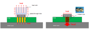
At the core of Copper Coin PCBs is the principle of thermal conductivity. Copper is one of the most thermally conductive materials available for PCB manufacturing, second only to silver. It has a thermal conductivity of approximately 400 W/m·K, which makes it ideally suited for transferring heat away from temperature-sensitive electronic components.
When embedded in a PCB, the copper coin serves as a direct thermal conduit. Unlike traditional thermal vias or copper planes that rely on indirect paths through dielectric layers and interfaces, a copper coin allows heat to flow directly from the component interface through a solid metal body. This significantly reduces the thermal resistance path and provides faster, more efficient heat dissipation.
3.2 Heat Transfer Mechanisms in Copper Coin PCBs
There are three main types of heat transfer relevant to PCB design: conduction, convection, and radiation. Copper Coin PCBs are primarily concerned with conduction, which involves the direct transfer of heat through solid materials.
In a standard PCB, conduction paths are interrupted by dielectric materials with low thermal conductivity, such as FR4, which typically has a thermal conductivity of only 0.3 W/m·K. In contrast, the insertion of a copper coin creates a high-efficiency conduction path between the heat-generating component and the opposite side of the board—or even directly to an attached heatsink or chassis. This path allows for:
-
Localized heat absorption: The copper coin acts as a heat spreader, absorbing heat directly from the component body.
-
Vertical thermal flow: Heat is transferred downward through the coin, bypassing multiple layers of dielectric material.
-
Lateral distribution: In larger copper coin designs, heat can also spread sideways across the plane of the board to reach auxiliary cooling structures.
This multi-directional heat management capability is what distinguishes Copper Coin PCBs from traditional thermal design approaches.
3.3 Reduction in Junction Temperature and Improved Component Lifespan
One of the most direct benefits of improved thermal management with Copper Coin PCBs is the reduction of junction temperature (Tj) in semiconductor devices. The junction temperature is the temperature at the point where the electrical activity occurs within a chip. Keeping Tj within specified limits is vital, as even small increases in temperature can significantly shorten component lifespan or cause operational instability.
For example, the Arrhenius equation suggests that for every 10°C increase in temperature, the lifespan of an electronic component may be halved. By lowering the Tj using efficient thermal pathways provided by a copper coin, devices can operate within their thermal budget, which extends service life, enhances reliability, and reduces failure rates.
3.4 Comparative Analysis: Copper Coin PCBs vs. Traditional Cooling Methods
Traditional PCB cooling techniques include the use of heatsinks, thermal pads, thermal vias, and thicker copper traces. While these methods have proven effective for many low-to-moderate power applications, they have inherent limitations:
| Cooling Technique | Thermal Path Efficiency | Space Requirements | Cost | Reliability in Harsh Environments |
|---|---|---|---|---|
| Thermal Vias | Medium | Minimal | Low | Moderate |
| Heatsinks | High (external) | High | Moderate to High | Low (prone to vibration issues) |
| Thick Copper Traces | Medium | Moderate | Moderate | Moderate |
| Copper Coin PCBs | Very High | Minimal | Moderate | Very High |
As shown in the comparison above, Copper Coin PCBs offer a superior balance between thermal performance and design efficiency. They deliver very high thermal transfer efficiency while consuming minimal additional space on the board, making them ideal for compact, high-performance applications.
3.5 Applications Where Thermal Management is Critical
There are numerous application areas where thermal control is not just desirable but absolutely essential. These include:
-
Power Electronics: High-efficiency converters and inverters used in EVs and renewable energy systems require precise thermal control to maintain operational integrity.
-
LED Lighting Systems: LEDs are extremely sensitive to heat; copper coin structures allow for improved thermal spreading, increasing brightness consistency and product life.
-
RF and Microwave Systems: Stability and frequency performance in RF systems can be degraded by temperature fluctuations, necessitating robust thermal designs.
-
Industrial Automation and Robotics: Motor controllers and high-current drivers generate significant heat, making effective dissipation crucial to prevent malfunction.
-
Data Centers and High-Performance Computing (HPC): Compact servers and processing units benefit from copper coin integration to manage heat within confined volumes.
3.6 Thermal Simulation and Design Validation for Copper Coin PCBs
Modern PCB design tools allow engineers to simulate thermal performance using finite element analysis (FEA) and computational fluid dynamics (CFD). These simulations provide predictive insights into how the heat will flow through the PCB, allowing designers to optimize the position, thickness, and material composition of copper coins.
In a typical design iteration, engineers may test multiple copper coin geometries and placements to see which configuration minimizes hotspot formation and evens out thermal gradients. This process helps achieve optimal cooling performance without excessive over-engineering or material waste.
Furthermore, once a prototype is fabricated, infrared thermography and embedded sensors can be used to validate the thermal performance of the copper coin in a real-world operating environment. These tools are essential in safety-critical systems where thermal margin validation is non-negotiable.
3.7 My Reflections on Thermal Engineering with Copper Coin PCBs
Having worked on multiple product designs where thermal constraints dictated the feasibility of the entire system, I have come to deeply appreciate the utility of embedded copper coins. Their implementation has repeatedly allowed our team to circumvent otherwise show-stopping thermal issues, particularly in products where adding external cooling components was either impractical or aesthetically unacceptable.
More importantly, copper coin designs challenge engineers to think in three dimensions—not just about signal traces and component footprints, but about the full thermal and mechanical interaction within the board. This depth of thinking leads to more robust, long-lasting products that meet the demands of today’s high-performance, compact, and environmentally challenging applications.
4. Electrical Performance Benefits of Copper Coin PCBs
In addition to their remarkable thermal advantages, Copper Coin PCBs offer significant enhancements in electrical performance. These improvements are particularly beneficial in high-speed, high-current, and high-frequency electronic applications, where signal integrity, power delivery, and electromagnetic compatibility are mission-critical. This section explores how the structural characteristics of Copper Coin PCBs contribute to superior electrical behavior and highlights the scenarios in which these features offer decisive engineering advantages.
4.1 Low Impedance Power Delivery in Copper Coin PCBs
In power-intensive applications, the delivery of consistent and stable current is essential. Traditional PCBs rely on copper planes and power vias to route energy to critical components. However, these methods introduce parasitic impedance, which can lead to voltage drops and inefficiencies, especially over long distances or under high current loads.
Copper Coin PCBs resolve this issue by providing a low-resistance, high-conductivity path from the power source directly to the component. This structure reduces voltage ripple and ensures minimal energy loss, which is particularly valuable for:
-
Power amplifiers
-
High-efficiency motor drivers
-
Voltage regulators
-
Battery management systems
The metal coin, being directly embedded and typically in contact with high-power pads, minimizes the resistive path length and effectively lowers the overall power distribution impedance of the system.
4.2 Enhanced Signal Integrity in Copper Coin PCBs
Signal integrity is increasingly vital in high-speed digital circuits. Issues such as signal reflection, crosstalk, and transmission delay become pronounced as clock speeds and edge rates increase. The integrity of the signal path depends largely on the consistency of the impedance and the minimization of noise sources.
Copper Coin PCBs contribute positively to signal integrity by:
-
Providing a stable reference plane: A large-area copper coin beneath high-speed signal lines can serve as a robust return path, ensuring consistent impedance.
-
Reducing inductive loop area: With a nearby ground or power plane embedded in copper, the loop area between signal and return is minimized, which reduces electromagnetic noise.
-
Shortening trace lengths: By placing copper coins near critical components, traces can be kept shorter and more direct, decreasing both resistance and inductance.
This structural advantage is crucial for systems such as high-speed memory buses, RF modules, and differential pair signaling in high-performance computing and communication applications.
4.3 Reduced Electromagnetic Interference (EMI) in Copper Coin PCBs
Electromagnetic interference (EMI) and electromagnetic compatibility (EMC) are major concerns in densely packed electronics, especially in automotive, aerospace, and IoT environments. Poor EMI control can result in erratic behavior, data corruption, or even regulatory non-compliance.
Copper Coin PCBs help mitigate EMI by:
-
Acting as an electromagnetic shield: The embedded metal coin can serve as an effective EMI barrier when connected to ground, particularly when placed underneath sensitive analog or high-speed digital components.
-
Improving grounding strategies: Multiple ground coins can be strategically positioned to create localized, low-impedance ground returns, suppressing high-frequency noise.
-
Enhancing decoupling performance: When placed near bypass capacitors, copper coins assist in stabilizing power delivery networks (PDNs), improving decoupling at critical nodes.
As a result, devices built with these boards often demonstrate improved compliance with EMC standards and reduced emissions in radiated and conducted tests.
4.4 Support for High-Frequency Performance in Copper Coin PCBs
Microwave and millimeter-wave systems demand precision in the control of transmission line characteristics such as characteristic impedance and loss tangent. At these frequencies, even minor discontinuities or mismatches in the board structure can degrade performance significantly.
Copper Coin PCBs support high-frequency signal performance through:
-
Minimized dielectric losses: By replacing part of the signal path with copper and minimizing lossy dielectric layers, signal attenuation is reduced.
-
Improved thermal stability: Thermal stability ensures that the dielectric constant (Dk) of the surrounding materials remains constant, avoiding signal phase shift or frequency drift.
-
Controlled impedance routing: The precise definition of coin location relative to signal layers enables better impedance matching over a wide frequency range.
These benefits make copper coin designs well-suited for radar systems, satellite transceivers, 5G antennas, and other high-frequency applications.
4.5 Impact on Current Carrying Capacity of Copper Coin PCBs
Current carrying capability is often limited by the width and thickness of copper traces on a PCB. As current increases, these traces heat up, potentially leading to reliability issues or failure if the thermal design is inadequate.
Copper Coin PCBs solve this by integrating massive cross-sectional metal elements directly into the board. This structure:
-
Supports very high currents (often in the tens or hundreds of amperes) without requiring excessively wide traces
-
Prevents localized overheating, thanks to the high thermal and electrical conductivity of the copper coin
-
Enables power distribution within compact designs, which would otherwise be limited by PCB layer count or trace routing constraints
This advantage is particularly useful in power distribution boards, DC-DC converters, and industrial controllers where large currents must be delivered reliably in a small form factor.
4.6 Copper Coin Integration and High-Speed PCB Stackup Design
Designing Copper Coin PCBs for optimal electrical performance requires careful integration into the board stackup. Key considerations include:
-
Coin placement relative to signal layers: To reduce loop inductance and support fast rise times
-
Isolation from noise-sensitive circuits: Ensuring that power coins do not interfere with analog or RF paths
-
Thermal-electrical dual optimization: Balancing current paths with thermal dissipation paths, especially when coins serve both roles
Modern PCB CAD tools support simulation of electrical behavior, including impedance modeling and current density analysis, to aid in copper coin design.
By embedding copper coins in carefully modeled locations, engineers can simultaneously achieve thermal and electrical performance goals without compromising board space or mechanical integrity.
4.7 Personal Insights into Electrical Engineering with Copper Coin PCBs
As someone involved in the development of high-power embedded systems, I’ve witnessed how even small changes in PCB layout can profoundly impact signal quality and power delivery. Integrating copper coins has offered a level of control and confidence that is difficult to replicate with conventional techniques.
For one project involving a multi-channel power amplifier array, we faced serious issues with thermal-induced impedance drift and erratic power rail behavior. The introduction of copper coins under each power stage drastically stabilized the performance, improved thermal handling, and suppressed EMI to within safe limits—all without increasing board dimensions. That experience reinforced for me how copper coin integration can serve as both a practical and strategic tool in advanced electronic system design.
5. Mechanical Strength and Structural Reliability of Copper Coin PCBs
Beyond thermal and electrical advantages, Copper Coin PCBs also bring notable improvements to the mechanical integrity and structural reliability of printed circuit boards. These qualities are increasingly important in industries such as aerospace, defense, and automotive electronics, where devices are subjected to mechanical vibration, shock, and harsh environmental conditions. This section examines how Copper Coin PCBs contribute to mechanical strength, long-term reliability, and structural robustness across demanding use cases.
5.1 Reinforcement Effect of Copper Coin PCBs in Mechanical Stress Environments
The inclusion of solid copper elements within the PCB substrate naturally enhances the rigidity and resistance of the board to mechanical deformation. In systems that encounter stress due to movement, shock, or uneven mounting pressure, traditional PCBs may warp or crack, especially when subject to prolonged load cycles.
Copper Coin PCBs counter this through:
-
Local reinforcement: The embedded copper coins act as rigid bodies, increasing stiffness in regions around high-stress components or connectors.
-
Load distribution: By spreading mechanical force over a wider area, copper coins help reduce point loading on delicate substrates.
-
Prevention of delamination: The solid interface between the coin and adjacent layers adds physical anchoring that resists layer separation under repeated flexing or vibration.
These enhancements significantly reduce mechanical failures in high-vibration environments such as vehicle dashboards, avionics, and industrial control units mounted on moving machinery.
5.2 Improved Resistance to Thermal Cycling in Copper Coin PCBs
Repeated heating and cooling cycles can cause thermal expansion and contraction of materials within a PCB. Over time, this leads to fatigue, cracking, or delamination—especially in via walls, solder joints, and around heat sources.
Copper Coin PCBs enhance resistance to thermal cycling by:
-
Reducing thermal gradients: The high thermal conductivity of the coin helps spread heat evenly, minimizing differential expansion between hot and cold regions.
-
Acting as mechanical anchors: Coins add mechanical strength at high-risk locations, resisting warping or separation between dielectric layers.
-
Enhancing solder joint reliability: Soldered components placed above or near a copper coin experience less thermal stress, as the coin dampens the expansion rate differences between materials.
This benefit is particularly valuable in systems subject to environmental fluctuations, such as outdoor telecommunications equipment or spacecraft electronics exposed to orbital temperature shifts.
5.3 Copper Coin PCBs for Shock and Drop Resilience
Consumer electronics and embedded devices often face sudden impact or drop events. Traditional PCBs can crack, delaminate, or lose solder joint integrity under such shocks—especially if the board has large unsupported areas or if components are mounted near edges or cutouts.
Copper Coin PCBs mitigate drop damage by:
-
Reinforcing weak zones: Placing a copper coin under mechanically sensitive regions (like connectors or inductors) can absorb and redistribute impact force.
-
Increasing local mass and stiffness: The coin’s presence adds density and rigidity, which dampens vibration and reduces bending during a drop.
-
Reducing PCB flexing: Since the board is less likely to bend, solder joint stress is reduced, leading to longer interconnect life even under repeated handling or transport.
This advantage is useful in handheld tools, ruggedized tablets, wearable electronics, and military field equipment.
5.4 Enhanced Screw Torque Resistance with Copper Coin PCBs
In mechanically fastened assemblies, such as those requiring metal standoffs or screws, localized pressure from tightening can damage standard PCB materials. Fracturing around screw holes or pad detachment is common when torque exceeds safe limits.
Copper Coin PCBs allow:
-
Placement of coins near mounting holes, where they distribute mechanical force more evenly through the board.
-
Direct screw insertion into plated coin structures, improving clamping force without cracking the board.
-
Higher allowable torque thresholds, which supports secure assembly in high-vibration or structural load scenarios.
This makes them ideal for automotive electronics, structural sensor modules, and power boards fastened into heavy industrial enclosures.
5.5 Long-Term Reliability of Solder Joints on Copper Coin PCBs
Solder joints are among the most common points of failure in electronic assemblies. Thermal expansion, vibration, and mechanical shock can all degrade solder integrity over time.
Copper Coin PCBs improve solder joint longevity by:
-
Reducing thermal fatigue: The coin’s mass stabilizes temperature fluctuations, preventing thermal cycling stress from repeatedly flexing solder joints.
-
Supporting heavier components: Components mounted above a coin are better supported, reducing mechanical leverage that could fracture joints.
-
Minimizing vibration effects: With reduced board flexing, vibration-induced micro-movements at the joint are minimized, extending joint life.
For example, in power electronics with heavy inductors or transformers, placing a copper coin beneath these components can drastically improve mechanical and electrical reliability.
5.6 Dimensional Stability in Harsh Environments with Copper Coin PCBs
Certain applications expose PCBs to extreme environmental stress—whether high humidity, vacuum, corrosive atmospheres, or mechanical abrasion. Under such conditions, maintaining dimensional accuracy is crucial, especially in systems where tight tolerances are required for RF performance or mechanical alignment.
Copper Coin PCBs assist in maintaining dimensional integrity by:
-
Anchoring key locations: Embedded metal features provide fixed structural points that reduce substrate warping or swelling.
-
Shielding against environmental stress: Coins can protect critical regions from moisture ingress or surface corrosion.
-
Retaining coplanarity: Boards with embedded coins resist bowing or twisting, which is important for systems that require tight enclosure fits or precise optical alignment.
This property is crucial for satellite payloads, sensor systems, and instrumentation exposed to atmospheric extremes or pressure variation.
5.7 Personal Reflection on Mechanical Reliability in Copper Coin PCBs
In my experience working with both military and high-power industrial applications, mechanical reliability is often undervalued during initial design—but proves vital in long-term deployment. I recall a project involving a motor controller embedded in a robotic arm. Initially, the team used conventional multilayer PCBs, but over time, the solder joints near power terminals failed due to cyclical mechanical strain and heat.
After switching to a design incorporating copper coins beneath the high-current connectors and mounting areas, the failure rate dropped to near zero. The board not only handled more current but also withstood shock and vibration from the robotic movements without degradation. That case convinced me that copper coin reinforcement isn’t just about thermal efficiency—it’s also about mechanical peace of mind.
6. Design Flexibility and Customization Potential of Copper Coin PCBs
One of the most compelling benefits that distinguishes Copper Coin PCBs from traditional board configurations is their inherent design flexibility and capacity for customization. In high-performance or constrained applications—such as aerospace, medical, and next-gen computing—engineers are increasingly tasked with crafting intricate power and signal paths that must also manage thermals, reduce losses, and withstand environmental extremes. Copper Coin PCBs offer a platform where standard constraints can be redefined through precision placement and tailored metallurgical integration. This section explores the myriad ways in which these PCBs expand creative and functional possibilities.
6.1 Custom Thermal Paths Enabled by Copper Coin PCBs
Unlike standard heat-dissipating layers that spread thermal energy uniformly, Copper Coin PCBs allow designers to create targeted, optimized thermal pathways:
-
Local thermal sinking: Coins can be inserted directly under high-heat components (e.g., MOSFETs, LEDs, processors) to channel heat vertically through the PCB to a heatsink or chassis.
-
Asymmetric heat paths: Custom shapes and thicknesses enable directional heat routing, bypassing temperature-sensitive circuitry.
-
Layer-specific integration: Designers can position coins in specific layers, accommodating both single- and multilayer strategies for managing heat without disturbing signal layers.
This freedom significantly benefits compact power modules and RF circuits, where thermal precision is paramount for performance consistency and lifespan.
6.2 Geometric Customization with Copper Coin PCBs
One remarkable aspect of Copper Coin PCBs is the degree to which the copper insert itself can be tailored geometrically. Unlike via arrays or thermal pads, which are often constrained by manufacturing toolsets, copper coins can be:
-
Cut into irregular or component-shaped geometries to match the footprint of custom ICs or module enclosures.
-
Designed with interlocks or notches to mechanically bind with the surrounding dielectric, improving anchoring.
-
Integrated with multiple thicknesses across the same board, creating multi-stage thermal resistance or capacitance profiles.
This geometric freedom supports complex 3D stacking, precise module fitting, and high-fidelity thermal modeling in the design stage.
6.3 Modular Placement Strategies in Copper Coin PCBs
Designers using Copper Coin PCBs are not limited to fixed configurations or symmetries. Placement strategies can be adjusted based on:
-
Functional zones: Specific regions can be hardened or cooled with coins, while others remain flexible or signal-focused.
-
Mechanical zones: Locations vulnerable to stress (e.g., around mounting holes, edge connectors, or touchpoints) can be selectively reinforced.
-
Multi-coin integration: Boards can incorporate several coins of varying shape, size, and alloy composition to optimize each functional block.
This modularity makes Copper Coin PCBs highly suitable for hybrid boards—combining RF, analog, digital, and power modules on a single platform without compromise.
6.4 Compatibility with Hybrid Material Systems in Copper Coin PCBs
Another advanced application is the integration of Copper Coin PCBs with exotic or hybrid base materials. These include:
-
High-frequency substrates (e.g., Rogers, Teflon composites) for 5G and microwave applications.
-
Ceramic or metal-core layers for ultra-high heat resistance or structural rigidity.
-
Flex-rigid systems, where coins are embedded only in the rigid zones while allowing the rest of the board to remain flexible.
This compatibility allows engineers to combine the best properties of multiple materials into one cohesive board, made possible by the targeted presence of copper coins.
6.5 Enhanced Power Distribution Design Using Copper Coin PCBs
In power-dense circuits, such as server backplanes, motor drivers, and energy inverters, the ability to deliver high currents efficiently is critical. Copper Coin PCBs support:
-
Low-resistance current paths: By placing coins beneath high-current traces or terminal blocks, voltage drop and heat generation are minimized.
-
Parallel power routing: Multiple coins can carry isolated or redundant power paths for fault tolerance.
-
Isolation barriers: Thick copper coins can also act as shielding planes or barriers between sensitive analog zones and noisy power circuits.
The control afforded by this level of customization can eliminate the need for bulky power planes or external copper bars, saving weight and volume.
6.6 Embedded Heat Sinks and Mechanical Anchors in Copper Coin PCBs
Copper coins in PCB designs can serve double duty—not only as thermal sinks but also as structural anchors for heavy or critical components. Their customization potential includes:
-
Machined surface profiles that allow direct soldering of packages or screw fasteners.
-
Multi-level stacking, where coins form interconnects between stacked boards or modules.
-
Integrated mounting supports, where the coin is extended or drilled to act as a structural bridge within an enclosure.
Such approaches allow PCBs to carry heavier loads and interface more securely with mechanical subsystems, which is essential in aerospace and vehicular applications.
6.7 Personal Reflection on Design Freedom with Copper Coin PCBs
From my own design experience in the fields of robotics and high-speed embedded computing, I’ve found that design freedom is often the gateway to innovation. In one prototype, we had a dense mix of power regulation, microcontroller, and communication logic all crammed into a small footprint. Managing EMI, heat, and mechanical stress simultaneously was nearly impossible—until we switched to a Copper Coin PCB.
We embedded a custom-shaped coin beneath the power section, which doubled as a localized heat sink and a current shunt. At the same time, the coin’s structural rigidity allowed us to mount the board using only two standoffs instead of four, freeing up precious real estate. That project showed me how copper coin integration doesn’t just solve thermal or mechanical challenges—it unlocks elegant, compact solutions that would otherwise require tradeoffs.
7. Application Scenarios Benefiting from Copper Coin PCBs
Copper Coin PCBs are particularly well-suited to industries and applications where high reliability, exceptional thermal performance, and efficient power delivery are crucial. By embedding solid copper elements within the PCB substrate, designers can develop boards that address unique environmental and electrical challenges across a variety of sectors. This section delves into specific industries and real-world use cases where the advantages of Copper Coin PCBs translate into measurable performance improvements.
7.1 Automotive Power Electronics and Copper Coin PCBs
The automotive industry increasingly relies on power electronics to support electric vehicle (EV) systems, advanced driver assistance systems (ADAS), and engine control units (ECUs). These applications often operate in environments with wide temperature swings, vibration, and high currents.
Copper Coin PCBs are particularly effective in:
-
Motor control modules, where copper coins enable better current flow and heat dissipation for high-power switches like IGBTs or MOSFETs.
-
Battery management systems (BMS), especially in EVs, where accurate thermal management is key to performance and safety.
-
Onboard chargers (OBCs), which demand high-frequency switching with minimal losses and localized cooling capabilities.
By embedding copper coins, automotive designers can reduce heat stress on components, maintain performance over longer periods, and improve overall system reliability.
7.2 Telecommunications Infrastructure and Copper Coin PCBs
As 5G and future 6G networks continue to expand, the demand for high-frequency, high-efficiency circuit boards increases. Base stations, antennas, and fiber-optic transceivers require stable thermal environments to operate at full capacity.
Copper Coin PCBs are applied in telecom infrastructure by:
-
Providing targeted thermal relief beneath high-power RF amplifiers and transceivers.
-
Supporting microwave PCBs with hybrid dielectric stacks, where embedded coins reduce interference and temperature-induced drift.
-
Enhancing backhaul power systems that use compact power conversion and filtering units.
These benefits translate to improved signal integrity, higher uptime, and lower failure rates in mission-critical networks.
7.3 Aerospace and Defense Applications of Copper Coin PCBs
Aerospace and defense systems frequently operate under extreme environmental conditions, including high altitudes, space vacuum, and intense vibration. Reliability is non-negotiable.
Copper Coin PCBs provide value in:
-
Flight control systems that must dissipate heat within constrained enclosures without active cooling.
-
Radar and RF communication modules, where thermal management ensures frequency stability.
-
Satellite electronics, where copper coins provide both thermal paths and mechanical reinforcement in radiation-hardened systems.
Additionally, copper coins allow better integration with metal-core PCBs or hybrid ceramic-based materials, which are common in space-grade electronics.
7.4 Medical Devices Leveraging Copper Coin PCBs
In the medical field, compact and high-performance electronics are essential for diagnostic, therapeutic, and surgical devices. Many of these systems require:
-
Precise temperature control, particularly in laser-based or RF-based treatment systems.
-
High-density component integration, such as in wearable monitors or implantable devices.
-
Longevity and reliability, with minimal failure over thousands of hours of use.
Copper Coin PCBs support these demands by allowing pinpointed heat removal, efficient signal routing, and mechanical stability—all within miniaturized form factors.
7.5 Industrial Automation and Power Systems with Copper Coin PCBs
Industrial environments expose PCBs to continuous stress from heat, dust, electrical surges, and mechanical vibrations. Systems like programmable logic controllers (PLCs), motor drives, and robotic controllers often experience:
-
Elevated operating temperatures, especially near power modules.
-
High-current switching, requiring robust copper traces.
-
Space constraints, where stacking or modular designs are used.
Copper Coin PCBs address these concerns by embedding copper directly under power semiconductors or connectors, minimizing voltage drops and ensuring consistent heat transfer even in closed enclosures.
7.6 LED Lighting and High-Performance Optoelectronics Using Copper Coin PCBs
Thermal performance is one of the key barriers to reliability in LED and optoelectronic devices. Without adequate heat dissipation, light output and color stability degrade rapidly.
Copper Coin PCBs play a pivotal role in:
-
High-power LED modules, where a coin acts as a direct thermal bridge from the diode to the heat sink.
-
Laser diode drivers, which are thermally and electrically sensitive and require isolated, low-inductance power delivery.
-
Camera modules and sensors, where localized heat buildup affects image quality or signal accuracy.
By precisely managing hot spots, copper coins allow designers to extend product lifespan, increase lumen efficiency, and improve optical consistency.
7.7 Renewable Energy Systems and Copper Coin PCBs
Solar inverters, wind turbine controllers, and battery storage modules are becoming more integrated and intelligent. This integration creates high thermal density in often inaccessible locations.
Copper Coin PCBs are applied in:
-
Solar MPPT controllers, where heat from high-frequency switches can cause efficiency losses.
-
Battery-to-inverter interface boards, which handle large currents and need to minimize conduction losses.
-
Hybrid energy systems, where mechanical robustness and thermal reliability are both needed for outdoor or mobile deployments.
In these applications, embedded copper coins make a noticeable difference in performance metrics and mean time between failures (MTBF).
7.8 Personal Reflection on Real-World Relevance of Copper Coin PCBs
From a practical engineering standpoint, I’ve seen how theory meets reality when deploying complex systems in harsh or unpredictable environments. One recent industrial project I worked on involved a smart sensor gateway that integrated a power module, real-time processor, and RF communications. The PCB needed to be compact, mountable on a vibrating motor chassis, and capable of handling continuous 4-amp loads.
Traditional multilayer boards quickly overheated or suffered delamination after thermal cycling. The adoption of a Copper Coin PCB resolved both thermal and mechanical challenges. We embedded two coins—one beneath the power module and one as a structural spine. Not only did it improve heat distribution, but it also reinforced the board mechanically, preventing microfractures from continuous vibration.
These experiences reinforce that the real-world advantages of Copper Coin PCBs go far beyond datasheets—they enable innovation in otherwise impossible scenarios.
8. Manufacturing Considerations for Copper Coin PCBs
Designing a high-performance Copper Coin PCB is only part of the challenge—the manufacturing process brings its own set of complexities that must be carefully addressed to fully realize the benefits of embedded copper technology. Unlike traditional multilayer PCBs, which rely solely on copper foils and plating, Copper Coin PCBs require precision machining, specialized lamination techniques, and careful thermal management during fabrication. This section explores the key production steps, challenges, and best practices that define successful implementation.
8.1 Material Preparation for Copper Coin PCBs
The foundation of manufacturing begins with selecting suitable materials for both the base laminate and the copper coins. The prepreg, core, and copper thickness must be chosen to match the thermal and electrical requirements of the design.
Key considerations include:
-
Base material: High-Tg FR4, ceramic-filled laminates, or metal-core substrates are often preferred for thermal durability.
-
Coin purity and finish: Oxygen-free copper (OFHC) with a smooth surface finish ensures excellent conductivity and bond strength.
-
Thickness uniformity: Since copper coins are relatively thick (typically 1.0–5.0 mm), strict thickness tolerances are necessary to avoid lamination defects.
Proper cleaning and preparation of both the board and coin surfaces are essential to promote adhesion and prevent delamination.
8.2 Routing and Pocket Milling for Copper Coin PCBs
A defining characteristic of Copper Coin PCBs is the pocket or cavity milled into the board core to receive the copper insert. This operation must be executed with extreme accuracy to ensure a proper mechanical fit.
Key process steps:
-
CNC routing or laser machining is used to create the cavity with tolerance levels typically within ±25 µm.
-
Depth control is critical, especially when coins must sit flush or protrude slightly for surface-mounted components.
-
Burr removal must be thorough to avoid stress concentrations or insulation layer damage during lamination.
In high-density boards, designers must carefully coordinate coin pocket locations with layer stack-up and internal via routing.
8.3 Coin Embedding Techniques in Copper Coin PCBs
The actual placement and bonding of the copper coin involve several precise steps that affect both the thermal and electrical characteristics of the board.
There are two primary methods:
-
Press-fit embedding, where the coin is inserted into the cavity and held by friction or minor interference before lamination.
-
Soldered or bonded embedding, where a thin solder layer or conductive epoxy is applied to enhance both thermal transfer and electrical contact.
Advanced approaches may involve plated-through copper coin embedding, where the coin is electrically connected to inner layers using plated vias or embedded traces.
8.4 Lamination and Heat Control in Copper Coin PCBs
Laminating a PCB that contains thick metal inserts requires adjustments to both pressure and temperature cycles. Standard lamination settings may be inadequate.
Best practices include:
-
Multi-stage lamination, using staggered heating ramps to reduce stress between copper and resin systems.
-
Vacuum-assisted lamination, which helps eliminate air bubbles or voids near the coin edge.
-
Heat sink integration, where the copper coin may also contact an external heat sink during curing to manage thermal gradients.
The mismatch in CTE (coefficient of thermal expansion) between copper and the laminate material must be accounted for during cooling to avoid cracking or warping.
8.5 Drilling and Via Management in Copper Coin PCBs
Once lamination is complete, the board must be drilled and plated. If vias are routed near or through the copper coin area, extra care is necessary.
Challenges include:
-
Tool wear from drilling through or adjacent to thick copper.
-
Risk of delamination at the coin interface if stress relief isn’t adequately designed.
-
Voiding and plating defects in vias that intersect coin boundaries.
Designers should avoid placing high-density via fields directly over coins and instead use staggered or offset layouts.
8.6 Surface Finishing and Planarity in Copper Coin PCBs
After the structural board is complete, the surface must be finished to allow for component assembly and soldering. For coins that serve as contact points or thermal pads, planarity is a significant concern.
Manufacturing steps involve:
-
Grinding or planarization to achieve flush alignment between the coin and the surrounding surface.
-
Surface treatment (ENIG, OSP, or immersion silver) to protect exposed copper and maintain solderability.
-
Masking or isolation, especially if the coin is not intended to be electrically active at the surface.
Coins that extend through the board or serve as thermal contacts must meet strict flatness tolerances, especially in high-power BGA or QFN packages.
8.7 Inspection and Testing of Copper Coin PCBs
Final testing of Copper Coin PCBs must go beyond conventional electrical continuity and shorts tests.
Special inspection methods include:
-
X-ray imaging, to verify the positioning and void-free lamination of the copper coin.
-
Thermal imaging or resistance measurement, to confirm thermal conductivity between components and the coin.
-
Pull testing, to evaluate the mechanical integrity of the coin’s interface, especially in vibration-prone environments.
In some cases, designers also perform accelerated life tests or thermal cycling tests to simulate long-term performance.
8.8 Personal Reflection on Manufacturing Realities of Copper Coin PCBs
From a hands-on manufacturing perspective, I’ve observed that success with Copper Coin PCBs often hinges not on a single process step, but on how well all steps align. In a previous industrial automation project, a high-efficiency motor controller failed several thermal tests despite meeting all electrical specs.
Postmortem analysis revealed that the coin had lifted slightly during lamination, introducing a tiny air gap. This gap wasn’t visible in X-rays but caused a 10°C increase in component temperature under load. We revised the process by adopting a vacuum lamination step and changing from press-fit to solder bonding. The result: consistent thermal contact and improved power output.
This experience underlines how critical it is to treat Copper Coin PCB manufacturing as a cohesive, iterative process. Small oversights can have big consequences, but when done right, the performance gains are substantial and lasting.
9. Cost and ROI Analysis of Copper Coin PCBs
Adopting new PCB technologies always invites scrutiny from both engineering and financial departments. The incorporation of embedded copper elements promises clear performance benefits, but these advantages come with associated costs. In this section, we will dissect the financial implications of implementing Copper Coin PCBs, examine both direct and indirect expenses, and analyze return on investment (ROI) in the context of thermal-critical applications.
9.1 Direct Material Costs in Copper Coin PCBs
The most apparent cost factor lies in the materials themselves. Copper coins—particularly high-purity variants like oxygen-free copper—are significantly more expensive per unit area than standard copper foil. Additionally, the thickness and mass of these inserts further raise the base material cost.
Key factors contributing to material cost:
-
Thickness of copper coin: Heavier coins demand more raw copper.
-
Purity and surface treatment: Coins may require plating, polishing, or oxidation prevention measures.
-
Compatibility with advanced laminates: High-Tg or metal-core substrates used in combination with copper coins also tend to carry premium pricing.
Despite the cost, many manufacturers accept this trade-off for the substantial thermal advantages in performance-critical applications.
9.2 Specialized Fabrication Processes for Copper Coin PCBs
Incorporating copper coins into PCB manufacturing necessitates non-standard processes. These specialized steps can significantly increase the cost per board, especially in low-to-medium production volumes.
Additional fabrication costs include:
-
CNC milling or laser routing to create precise coin pockets.
-
Advanced lamination techniques such as vacuum-assisted or multi-stage lamination.
-
Manual or semi-automated coin insertion which slows down throughput and increases labor intensity.
-
Post-lamination grinding to ensure coin planarity.
Yield loss is also more likely in the early stages of adopting this technology, further adding to initial production costs.
9.3 Equipment and Tooling Considerations for Copper Coin PCBs
Investment in new or modified tooling is often necessary when transitioning to Copper Coin PCBs. Manufacturers may need to upgrade or supplement their fabrication lines.
Key equipment upgrades:
-
Precision CNC routers capable of maintaining micron-level depth tolerances.
-
Vacuum lamination presses to avoid delamination or voids near coin interfaces.
-
Metrology tools such as laser profilometers or x-ray inspection systems.
Initial capital expenditures can be considerable, but for high-volume production, these investments may be amortized over time.
9.4 Reliability-Driven Savings from Copper Coin PCBs
One of the most compelling arguments in favor of Copper Coin PCBs is their potential to reduce downstream failure rates, repair costs, and warranty claims.
Benefits contributing to long-term savings:
-
Improved heat dissipation extends component lifespan.
-
Lower junction temperatures improve IC reliability and reduce the risk of thermal runaway.
-
Fewer thermal vias or external heat sinks needed, simplifying BOM and assembly.
These reliability improvements are particularly valuable in mission-critical industries such as aerospace, electric vehicles, and industrial automation.
9.5 Performance ROI of Copper Coin PCBs in High-Stakes Applications
While the upfront cost of implementing Copper Coin PCBs is undeniably higher, the performance gains in some cases justify the expenditure entirely.
Consider these use cases:
-
High-current motor controllers: Copper coin integration can allow for smaller board sizes or higher current capacity, leading to system-wide cost savings.
-
LED lighting modules: Enhanced heat spreading reduces the need for bulky aluminum backings or forced air cooling.
-
Automotive electronics: Improved thermal performance increases product longevity, aligning with stringent lifecycle expectations.
In many scenarios, the ROI is measured not just in reduced failures, but also in enhanced competitiveness, enabling product features that would otherwise be thermally constrained.
9.6 Volume Scaling and Cost Curve Flattening of Copper Coin PCBs
Initial production runs of Copper Coin PCBs are typically cost-prohibitive due to NRE (non-recurring engineering) and setup fees. However, as volumes increase and processes mature, the unit cost can decline appreciably.
Drivers of cost reduction over time:
-
Process optimization: Tighter process control reduces scrap and rework.
-
Design standardization: Reusing coin shapes or board layouts across products lowers complexity.
-
Economies of scale: Bulk material purchases and longer machine runtimes reduce per-unit overhead.
Long-term, manufacturers often find that copper coin integration can be cost-competitive with alternative thermal solutions when properly implemented.
9.7 Hidden Costs and Pitfalls in Copper Coin PCBs
While most discussions focus on visible costs, hidden costs must also be evaluated to avoid unpleasant surprises.
Potential hidden costs:
-
Extended prototyping cycles due to complex thermal modeling and mechanical validation.
-
Training and yield loss during the transition phase for production teams.
-
Longer lead times when outsourcing to vendors unfamiliar with copper coin integration.
These risks can be mitigated with clear communication, early design for manufacturability (DFM) analysis, and supplier collaboration.
9.8 Reflecting on Financial Strategy in Copper Coin PCBs Adoption
In my experience working with mid-sized electronics firms, one common pitfall is focusing too heavily on the initial cost per board without fully accounting for the system-level cost or long-term savings.
In one project, a team rejected copper coin designs in favor of traditional PCBs with thermal vias and external heat sinks. Though the initial savings were about 12%, the final product required costly redesigns and field replacements due to thermal failures. Eventually, the switch to Copper Coin PCBs yielded a 38% improvement in thermal reliability and a measurable drop in warranty service calls.
This highlighted a key lesson: investing in advanced PCB structures like copper coin integration may seem expensive upfront, but often pays off dramatically over the product lifecycle—especially in thermally demanding use cases.
10. Future Trends and Research in Copper Coin PCBs
As electronics continue to evolve toward higher power densities, miniaturization, and greater reliability, Copper Coin PCBs stand poised for increased adoption and innovation. This final section examines emerging trends, ongoing research, and potential future developments shaping the landscape of Copper Coin PCBs. Understanding these trajectories is essential for engineers, manufacturers, and designers aiming to leverage copper coin technology effectively in next-generation applications.
10.1 Advances in Material Science for Copper Coin PCBs
Material science innovations are critical drivers enabling the next phase of Copper Coin PCB evolution. Researchers are exploring novel substrate materials, surface treatments, and copper alloys to enhance both thermal and mechanical performance.
Highlights include:
-
Nano-enhanced laminates with improved thermal conductivity while maintaining dielectric strength.
-
Copper alloys with tailored coefficients of thermal expansion to better match adjacent substrates, reducing stress.
-
Advanced coatings that prevent oxidation without compromising solderability or conductivity.
These breakthroughs promise to push the operational limits of copper coin-embedded PCBs in harsh environments such as automotive under-hood electronics and aerospace avionics.
10.2 Integration with Emerging PCB Technologies
Copper Coin PCBs do not exist in isolation but can synergize with other cutting-edge PCB manufacturing methods.
Examples of integration include:
-
Embedded heat pipes or vapor chambers combined with copper coins for ultra-efficient heat dissipation.
-
Additive manufacturing techniques (e.g., 3D printing of conductive materials) enabling more complex coin geometries and tailored thermal pathways.
-
Flexible and rigid-flex Copper Coin PCBs that bring the thermal benefits of copper coins to bendable substrates used in wearable or implantable devices.
By converging these technologies, engineers can achieve unprecedented thermal management solutions in compact form factors.
10.3 Simulation and Modeling Enhancements for Copper Coin PCBs
Thermal and mechanical simulation tools continue to advance, providing deeper insights into Copper Coin PCB behavior during operation and fabrication.
Key trends include:
-
Multi-physics simulation platforms that combine thermal, structural, and electromagnetic analyses.
-
Machine learning models trained on manufacturing data to predict defect rates or optimize lamination parameters.
-
Real-time monitoring integration, where sensors embedded near copper coins provide live thermal feedback during product use.
These tools accelerate design cycles and reduce prototyping costs by enabling precise prediction of copper coin performance.
10.4 Environmental and Sustainability Considerations
As sustainability becomes a priority, the environmental impact of PCB manufacturing, including Copper Coin PCBs, is under increasing scrutiny.
Relevant research focuses on:
-
Recyclability of copper coins and composite boards, aiming to reduce waste in end-of-life electronics.
-
Lower energy lamination processes to decrease carbon footprints during production.
-
Alternative, eco-friendly materials that preserve performance while minimizing environmental harm.
Such efforts are crucial to align Copper Coin PCB technology with global sustainability goals and regulatory trends.
10.5 Emerging Applications Driving Copper Coin PCB Innovation
New application domains are accelerating demand and innovation in Copper Coin PCB design.
Prominent sectors include:
-
Electric vehicles (EVs), where power electronics require enhanced thermal paths for safety and efficiency.
-
5G infrastructure and data centers, needing reliable high-power boards with superior heat spreading.
-
Medical devices, particularly implantables and wearables, where thermal management ensures patient safety and device longevity.
These fields push for thinner, lighter, and more efficient Copper Coin PCBs, spurring creative design and fabrication methods.
10.6 Industry Collaboration and Standardization Efforts
The rapid evolution of Copper Coin PCBs is fostering greater collaboration between material suppliers, PCB manufacturers, and end-users.
Ongoing initiatives involve:
-
Developing industry standards for copper coin dimensions, tolerances, and testing protocols to ensure interoperability and quality.
-
Joint research programs exploring novel integration techniques and reliability testing methods.
-
Knowledge-sharing platforms where case studies and best practices are disseminated to accelerate adoption.
Standardization will play a key role in scaling Copper Coin PCB technology across diverse markets.
10.7 Personal Insights on the Future of Copper Coin PCBs
Reflecting on current trends and conversations with industry experts, it’s clear Copper Coin PCBs are moving from niche solutions toward mainstream technology. The balance of cost, performance, and reliability will improve as processes mature and materials advance.
From my perspective, one exciting frontier is the convergence of Copper Coin PCBs with embedded sensors and smart monitoring. Imagine boards that not only manage heat effectively but also provide real-time data on thermal stresses and aging, enabling predictive maintenance and longer product lifetimes.
This integration aligns perfectly with the broader Industry 4.0 vision and smart manufacturing trends, promising a future where Copper Coin PCBs are central to truly intelligent electronic systems.
11. Conclusion on the Pros of Copper Coin PCBs
In this comprehensive exploration of the pros of Copper Coin PCBs, we have examined their fundamental characteristics, thermal performance benefits, mechanical advantages, electrical improvements, and financial implications. As a technology, Copper Coin PCBs stand out by offering superior heat dissipation, enhanced reliability, and design flexibility, addressing some of the most pressing challenges in modern high-power and high-density electronic applications.
11.1 Summarizing the Key Advantages of Copper Coin PCBs
Throughout this article, the major benefits of Copper Coin PCBs have been highlighted:
-
Enhanced thermal management: Copper coins serve as efficient heat spreaders, significantly reducing hotspot temperatures and preventing thermal failures.
-
Mechanical robustness: The embedded copper elements improve structural integrity and resistance to mechanical stress.
-
Electrical performance: Copper coins contribute to reduced impedance and signal interference in certain designs.
-
Design adaptability: The technology allows for innovative solutions such as localized cooling and hybrid substrate integration.
-
Reliability improvements: Lower operating temperatures translate to longer component life and reduced failure rates.
-
Cost-benefit considerations: Despite higher initial costs, the total cost of ownership often decreases due to improved performance and reduced warranty claims.
11.2 Reflecting on Practical Considerations
Adopting Copper Coin PCBs requires careful consideration of fabrication complexities, supply chain readiness, and design integration. Manufacturers must invest in tooling, training, and process optimization to realize the full potential of this technology. Moreover, early-stage collaboration between design and manufacturing teams can mitigate risks and improve yield.
11.3 Personal Reflections and Final Thoughts
In my experience, Copper Coin PCBs represent a strategic investment that pays dividends in applications where thermal management is critical. The evolving ecosystem around this technology, including material advances and simulation tools, is making it increasingly accessible and effective.
Looking forward, I believe Copper Coin PCBs will become a cornerstone technology in the development of next-generation electronics that demand both compactness and reliability. Their unique combination of thermal, mechanical, and electrical benefits positions them well to meet the challenges of emerging applications from automotive to aerospace to consumer electronics.
11.4 Encouraging Adoption and Innovation
I encourage engineers and designers to explore Copper Coin PCBs not just as a niche option but as a mainstream solution for thermal challenges. Continued innovation, standardization, and knowledge sharing will be essential to unlocking the full advantages of this promising technology.

- long board pcb
- Flexible PCBs
- Special PCB
- Express Printed Circuit Board
- Pcb Prototype
- LED PCB
- PCB
- Printed Circuit Board
- Pcb meaning
- Pcb manufacturer
- Rigid pcb board
- Rigid Flex PCB
 Quote
Quote
 E-mail