Introduction to BGA Substrate
1.1 What is a BGA-Substrate?
A BGA substrate (Ball Grid Array substrate) is a crucial component in semiconductor packaging, providing mechanical and electrical connections between an integrated circuit (IC) and a printed circuit board (PCB). This packaging technology has gained widespread adoption due to its high-density interconnection capability, superior thermal performance, and reliability.
1.2 Importance of BGA-Substrate in Modern Electronics
With the rapid advancement in semiconductor technology, BGA substrates play an essential role in miniaturizing electronic devices while maintaining high performance. They are widely used in applications such as high-performance computing, telecommunications, automotive electronics, and consumer devices.
1.3 Evolution of BGA-Substrate Technology
The development of BGA substrates has progressed significantly over the past decades. Early PCB-based packaging solutions were replaced with more advanced organic and ceramic substrates. The introduction of flip-chip BGA substrate (FCBGA) and embedded die packaging has further improved electrical and thermal performance, paving the way for more sophisticated electronic applications.
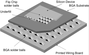
BGA Substrate
2. Types of BGA-Substrate
2.1 Ceramic BGA-Substrate (CBGA)
A ceramic BGA-substrate is made from multi-layered ceramic materials, offering excellent thermal stability and mechanical strength. It is often used in high-reliability applications such as aerospace, military, and high-performance computing.
2.2 Plastic BGA-Substrate (PBGA)
A plastic BGA-substrate consists of organic materials, such as epoxy resin and fiberglass. It is more cost-effective than ceramic substrates and is widely used in consumer electronics. However, it has limitations in thermal performance.
2.3 Tape BGA-Substrate (TBGA)
A tape BGA substrate uses a thin, flexible tape as the base material, making it suitable for lightweight and compact electronic devices such as smartphones and wearables.
2.4 Flip-Chip-BGA Substrate (FCBGA)
A flip-chip BGA substrate allows the IC to be directly mounted onto the substrate with its active side facing down. This configuration shortens interconnection lengths, reduces signal loss, and enhances high-frequency performance.
2.5 Embedded BGA-Substrate
Recent advancements have led to embedded BGA substrates, where components such as passive resistors and capacitors are integrated within the substrate layers. This approach reduces footprint, enhances reliability, and improves electrical performance.
3. Materials Used in BGA-Substrate
3.1 Organic BGA-Substrate Materials
Organic BGA substrates are made from epoxy resins reinforced with glass fibers. These materials offer flexibility and cost-effectiveness but may require additional processing to enhance thermal and electrical properties.
3.2 Ceramic BGA Substrate Materials
Ceramic BGA substrates are composed of materials such as alumina (Al₂O₃) and aluminum nitride (AlN), which provide superior heat dissipation and mechanical strength.
3.3 Build-Up Substrate Materials
Build-up BGA-substrates use multiple layers of dielectric and conductive materials, allowing for high-density interconnects and complex circuit designs.
3.4 Advanced-Substrate Materials
With the increasing need for higher performance, manufacturers are exploring low-loss laminates, embedded capacitors, and high-frequency materials such as PTFE (polytetrafluoroethylene) and Rogers laminates.
4. BGA Substrate Manufacturing Process
4.1 Core Formation in BGA Substrate
The core of a BGA-substrate is formed by laminating multiple layers of insulating and conductive materials. Vias are drilled and plated with copper to establish electrical connections.
4.2 Build-Up Layers for High-Density BGA Substrate
Advanced BGA substrates require multiple build-up layers to accommodate high-density interconnections. Techniques such as laser drilling and electroplating are employed.
4.3 Surface Finishing of BGA-Substrate
Common surface finishes for BGA substrates include:
- Electroless Nickel Immersion Gold (ENIG) – Provides good corrosion resistance and solderability.
- Organic Solderability Preservatives (OSP) – A cost-effective method for protecting copper pads.
- Electrolytic Gold Plating – Used for high-reliability applications.
4.4 Quality Control and Testing in BGA-Substrate Manufacturing
Stringent quality control measures, such as Automated Optical Inspection (AOI) and X-ray inspection, ensure the reliability of BGA substrates.
5. BGA-Substrate Design Considerations
5.1 Electrical Performance of BGA-Substrate
To maintain high electrical performance, BGA-substrate design must consider factors such as:
- Impedance control
- Signal integrity
- Crosstalk minimization
5.2 Thermal Management for BGA-Substrate
Heat dissipation is a critical factor in BGA-substrate design. Effective thermal management techniques include:
- Thermal vias
- Heat sinks
- High thermal conductivity materials
5.3 Mechanical Reliability of BGA-Substrate
Ensuring mechanical reliability in BGA-substrates requires:
- Optimizing solder ball geometry
- Minimizing warpage
- Matching material coefficients of thermal expansion (CTE)
6. Applications of BGA-Substrate
6.1 BGA Substrate in Consumer Electronics
BGA substrates are used in smartphones, tablets, and gaming consoles due to their ability to support high I/O densities in compact designs.
6.2 BGA Substrate in Telecommunications
In telecommunications, BGA substrates enable high-speed data transmission in network switches, base stations, and routers.
6.3 BGA Substrate in Automotive Electronics
Advanced driver-assistance systems (ADAS) and engine control units (ECUs) rely on BGA substrates for robust performance in harsh environments.
6.4 BGA Substrate in Industrial and Medical Devices
High-reliability BGA substrates are used in industrial automation and medical imaging systems.
7. Future Trends in BGA Substrate Technology
7.1 Miniaturization and High-Density Packaging
The demand for smaller, more powerful electronic devices is driving advancements in BGA substrate technology. Ultra-fine pitch and multi-layer designs are becoming standard.
7.2 Enhanced Thermal Solutions for BGA Substrate
Future BGA substrates will incorporate advanced cooling techniques, such as embedded heat spreaders and thermal vias.
7.3 5G and AI Integration with BGA Substrate
The adoption of 5G and AI-driven applications requires BGA substrates with higher-frequency capabilities and lower signal loss.
7.4 Sustainable and Lead-Free BGA Substrate Manufacturing
Environmental concerns are pushing for lead-free and RoHS-compliant BGA substrate manufacturing processes.
8. Challenges in BGA Substrate Manufacturing
While BGA substrate technology has evolved significantly, manufacturers still face several challenges that impact cost, reliability, and performance. Addressing these challenges is critical to improving the quality of BGA substrates and ensuring their successful deployment in high-performance applications.
8.1 Warpage in BGA-Substrate
One of the primary challenges in BGA-substrate manufacturing is warpage. Due to the mismatch in thermal expansion coefficients between different materials, warping can occur during the reflow soldering process. Excessive warpage can lead to solder joint defects such as open circuits and cold soldering.
Solutions to Reduce Warpage:
- Material selection: Using low-CTE (Coefficient of Thermal Expansion) substrate materials to minimize thermal expansion differences.
- Optimized layer stacking: Implementing balanced copper distribution and symmetric layer designs to reduce mechanical stress.
- Process control: Applying precise temperature profiles during reflow soldering to control expansion and contraction rates.
8.2 Solder Joint Reliability in BGA-Substrate
As electronic devices become more compact, solder joint reliability in BGA-substrates is a growing concern. High-density interconnections are more prone to thermal cycling fatigue, mechanical stress, and electromigration.
Strategies to Improve Solder Joint Reliability:
- Using underfill materials: Underfill helps distribute stress and enhance solder joint strength.
- Enhanced solder alloys: Implementing lead-free solder alloys with better mechanical properties.
- Fine-pitch optimization: Adjusting ball pitch and pad design to improve solderability.
8.3 Signal Integrity and High-Frequency Performance
With the rise of 5G, AI, and high-speed computing, ensuring good signal integrity in BGA-substrates is crucial. Signal degradation due to impedance mismatch, crosstalk, and electromagnetic interference (EMI) can severely affect performance.
Best Practices for Signal Integrity Optimization:
- Impedance control: Designing traces with proper widths, dielectric materials, and layer stack-ups to maintain impedance matching.
- Reducing via stubs: Using back-drilled vias or blind/buried vias to reduce reflections and signal loss.
- Shielding techniques: Implementing ground planes and isolation structures to minimize EMI effects.
8.4 Thermal Management in BGA-Substrate
High-power applications demand effective thermal management strategies to prevent overheating and ensure long-term reliability. BGA-substrates used in AI processors, GPUs, and networking equipment generate significant heat, requiring efficient cooling techniques.
Techniques for Improved Thermal Performance:
- Integrating thermal vias: Placing thermally conductive vias under the die to dissipate heat efficiently.
- Utilizing heat spreaders: Adding copper or aluminum layers to distribute heat away from critical components.
- Adopting high-Tg materials: Using high-glass transition temperature (Tg) laminates to withstand elevated temperatures.
9. Reliability Testing for BGA-Substrate
To ensure that BGA-substrates meet stringent industry standards, extensive reliability testing is required. These tests assess durability, electrical performance, and mechanical robustness under real-world conditions.
9.1 Thermal Cycling Test (TCT)
Thermal cycling is performed to evaluate the effects of temperature fluctuations on solder joints and substrate materials. The test subjects the BGA-substrate to repeated heating and cooling cycles, simulating operational environments.
Key Metrics:
- Number of cycles before failure
- Crack propagation in solder joints
- Delamination in multilayer substrates
9.2 Highly Accelerated Stress Test (HAST)
HAST is used to accelerate moisture-induced failures in BGA-substrates. High humidity and temperature conditions are applied to assess the reliability of the package under extreme environmental conditions.
Failure Modes Observed:
- Corrosion of interconnects
- Delamination of substrate layers
- Dielectric breakdown due to moisture absorption
9.3 Drop and Shock Testing
For mobile and consumer electronics, drop tests simulate the impact forces experienced during accidental falls. This test is essential for evaluating the mechanical robustness of BGA-substrates.
Parameters Evaluated:
- Solder joint integrity after impact
- Substrate cracking and chipping
- Electrical continuity after multiple drops
9.4 Electromigration and Aging Tests
Long-term exposure to high current densities can lead to electromigration, which degrades interconnects over time. Aging tests are conducted to assess the BGA-substrate’s performance under prolonged electrical stress.
10. Advanced Technologies in BGA-Substrate Design
10.1 2.5D and 3D Packaging for BGA-Substrate
The evolution of semiconductor packaging has led to 2.5D and 3D IC integration, where multiple dies are stacked on a single BGA-substrate. These technologies improve data transfer speeds and reduce latency in high-performance computing applications.
Advantages of 2.5D and 3D Packaging:
- Higher interconnect density
- Reduced power consumption
- Improved signal integrity
10.2 Embedded Passives in BGA-Substrate
To minimize board space and enhance electrical performance, passive components such as resistors and capacitors are embedded within the BGA-substrate itself.
Benefits of Embedded Passives:
- Lower parasitic inductance
- Enhanced power distribution network (PDN) stability
- Reduced overall footprint
10.3 AI-Driven Design Optimization for BGA-Substrate
With the rise of artificial intelligence (AI), BGA-substrate design is increasingly relying on AI-driven simulations and machine learning algorithms. These technologies help in:
- Predicting manufacturing defects
- Optimizing layer stack-ups for better signal integrity
- Automating layout generation for high-density designs
11. Future Trends in BGA-Substrate Technology
11.1 Adoption of Advanced Materials
The use of high-speed, low-loss materials will continue to grow as demand for high-frequency applications increases. Future BGA-substrates may incorporate materials such as:
- Liquid crystal polymer (LCP) for high-frequency performance
- Graphene-based conductors for improved thermal conductivity
- Flexible substrates for wearable and foldable electronics
11.2 Integration of Optical Interconnects
To address the limitations of electrical interconnects, BGA-substrates with integrated optical waveguides are being developed. These substrates enable ultra-high-speed data transmission with minimal signal loss.
11.3 Sustainability in BGA-Substrate Manufacturing
With stricter environmental regulations, manufacturers are focusing on:
- Lead-free soldering and RoHS-compliant materials
- Recyclable substrates to reduce electronic waste
- Energy-efficient manufacturing processes
Conclusion
As electronic devices continue to evolve, BGA-substrate technology will play a pivotal role in enabling high-performance computing, advanced telecommunications, and miniaturized consumer electronics. Ongoing research in materials, manufacturing techniques, and thermal management solutions will further enhance the capabilities of BGA-substrates, making them indispensable in next-generation applications.

 Quote
Quote
 E-mail