1. Introduction to Backdrill PCB
In the rapidly evolving field of printed circuit board (PCB) design, signal integrity, high-speed data transmission, and precise impedance control are more critical than ever before. Among the numerous techniques and technologies developed to address these demands, Backdrill PCB has emerged as a powerful solution for reducing signal stubs and improving overall board performance. Despite being a relatively specialized process, backdrilling has gained widespread traction, particularly in applications that require extremely high data integrity, such as telecommunications, aerospace, data centers, and 5G networks.
Understanding the Context of Backdrill PCB
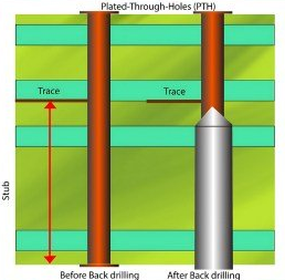
Before diving into the intricacies of the Backdrill PCB, it’s essential to appreciate the core problem it addresses: via stubs. In multi-layer PCBs, especially those designed for high-frequency signals, plated through holes (PTHs) often extend beyond the layers that require electrical connection. This leftover segment—known as a stub—can act as a parasitic antenna, introducing unwanted signal reflections, delay, and even data loss. The backdrilling process removes these stubs by mechanically drilling them out after the initial hole plating and layer interconnection have been established.
The Strategic Significance of Backdrill PCB
The application of a Backdrill PCB isn’t a random design choice. It is a strategic engineering decision aimed at optimizing signal flow, reducing jitter, and enhancing performance at GHz-level frequencies. As the industry shifts toward designs with tighter constraints and thinner margins of error, backdrilling has become an increasingly essential tool in the PCB engineer’s arsenal.
The rise of technologies like PCIe Gen 4/5, Ethernet 25G/40G/100G, and high-speed DDR memory makes the Backdrill PCB not just an advanced feature, but often a requirement for compliance with performance standards.
Why Backdrill PCB is Still Underutilized
Interestingly, many design engineers still treat the Backdrill PCB as an exotic or unnecessary addition to the stackup, largely due to limited familiarity with the process or concerns over cost and complexity. However, as more design teams embrace simulation-driven design flows and SI/PI (Signal Integrity / Power Integrity) analysis, the role of backdrilling is gaining visibility. For those who understand its value, it becomes not only a performance enhancer but a differentiator in PCB competitiveness.
My Thoughts: Why Backdrill PCB Matters More Today Than Ever
From my perspective, the increasing demand for higher bandwidth and lower noise in nearly all sectors of electronics makes backdrilling a non-negotiable consideration in many designs. Years ago, signal reflections due to stubs might have gone unnoticed or had minimal impact, especially in consumer-grade electronics. Today, even small mismatches can lead to catastrophic failures in data-driven applications. Backdrilling, when used effectively, can be the key to unlocking the full performance potential of your multilayer PCB designs.
Moreover, I believe that backdrill technology is part of a broader paradigm shift in PCB design philosophy. We’re no longer just routing traces to connect components; we’re now shaping electromagnetic pathways with scientific precision. That’s the world in which the Backdrill PCB operates—a world where precision equals performance.
Backdrill PCB
2. Historical Background and Evolution of Backdrill PCB
The development of Backdrill PCB technology is closely tied to the broader evolution of multilayer printed circuit boards and the demands of high-speed electronics. To understand why backdrilling has become such a critical design and manufacturing practice, it’s useful to examine its historical trajectory. From early PCB innovations to modern high-frequency circuit designs, backdrill technology has evolved in response to very specific electrical challenges.
The Early Days: From Basic PCBs to Complex Layer Stacks
The earliest printed circuit boards, dating back to the 1940s and 1950s, were single-layer constructions with minimal requirements in terms of signal integrity. As electronics grew more sophisticated—particularly in computing and telecommunications—engineers began stacking layers to create more complex routing architectures. By the 1980s and 1990s, multilayer PCBs with ten or more layers became commonplace in servers, routers, and radar systems.
However, with increased layering came the problem of via stubs—unused portions of plated through holes that created signal reflections and electromagnetic interference. At this stage, few solutions existed. Engineers primarily relied on clever routing strategies and signal termination methods, but the problem persisted as data speeds climbed.
The Emergence of Backdrill PCB as a Targeted Solution
The concept of Backdrill PCB gained real momentum in the early 2000s. With digital signaling rates climbing beyond 2.5 Gbps, traditional PTHs began acting as antennas, severely degrading signal performance. Engineers observed that via stubs acted as resonance points, introducing reflections that interfered with both rising and falling signal edges. It was during this period that mechanical backdrilling was introduced as a method to remove unused via segments and improve signal fidelity.
Initially, the adoption of backdrilling was limited to military and aerospace sectors, where performance was prioritized over cost. Over time, as commercial networking equipment—like Ethernet switches and routers—moved into the multi-Gbps range, the Backdrill PCB approach began to spread across industrial and enterprise markets.
Standardization and Tooling Advancements in Backdrill PCB
The mid-to-late 2000s saw significant improvements in CNC drilling technology and inspection methods, making backdrilling more feasible and cost-effective. PCB fabricators began offering automated backdrill services, incorporating high-precision registration systems and depth control mechanisms.
During this period, organizations such as IPC (Institute for Printed Circuits) began establishing guidelines for stub removal and signal integrity practices. As a result, Backdrill PCB techniques gained formal recognition and integration into broader Design for Manufacturing (DFM) and Design for Signal Integrity (DfSI) workflows.
Recent Years: Mainstream Adoption of Backdrill PCB in High-Speed Designs
In the last decade, the technology landscape has undergone a seismic shift. The transition to PCIe Gen 4/5, 100G Ethernet, DDR4/DDR5, and 5G millimeter-wave systems has dramatically elevated performance requirements. Today, Backdrill PCB techniques are no longer confined to mission-critical applications—they are used across a wide array of commercial products where clean signal paths are paramount.
Major OEMs now include backdrilling as part of their standard PCB design reviews, especially for high-speed serial links, differential pairs, and clock routing. Software tools like Altium Designer, Cadence Allegro, and Mentor Xpedition provide backdrill planning features, enabling simulation and design rule checks directly within the layout environment.
Personal Reflection: The Evolution of Backdrill PCB Mirrors Our Shift to Precision Electronics
From my viewpoint, the historical development of Backdrill PCB encapsulates a broader narrative: the transformation of electronics from functional interconnection platforms into precision-tuned systems. The evolution of backdrilling technology reflects our growing understanding of high-frequency physics and our commitment to controlling variables once considered minor nuisances.
As an engineer or designer today, ignoring via stubs is no longer an option. The lessons of the past—especially the harsh realities of signal degradation—have taught us that even microscopic design oversights can have macroscopic consequences. The journey of Backdrill PCB from obscurity to mainstream use illustrates how innovation arises not from flashy breakthroughs, but from methodical engineering refinement.
3. Technical Definition and Structure of Backdrill PCB
To effectively use a Backdrill PCB, engineers must understand not only its purpose but also its structure and how it integrates within the broader architecture of a multilayer PCB. Backdrilling is a mechanical post-processing technique that is applied after a standard plated-through-hole (PTH) via is formed and electroplated. Its purpose is to selectively remove the unused stub portion of the via to enhance electrical performance, particularly in high-speed digital and RF applications.
What Is a Backdrill PCB – A Technical Definition
A Backdrill PCB refers to a printed circuit board that has undergone the backdrilling process, in which via stubs are drilled out from the non-functional portion of a plated through-hole. These stubs are the segments of the via that do not carry electrical signals but remain part of the physical drilled hole and plated structure. Because these stubs can cause signal reflection and resonance at high frequencies, backdrilling is employed to eliminate them.
In simple terms, a backdrilled via is a non-blind through-hole where the electrical connection stops before reaching the far end of the hole, and that remaining part is drilled out after plating. The result is a via that connects only the necessary layers, with the remaining plated segment—called the stub—mechanically removed to improve performance.
Structure of a Backdrill PCB via
The anatomy of a Backdrill PCB via includes the following elements:
-
Barrel (Conductive Wall): The cylindrical plated wall formed during the through-hole plating process.
-
Pad Connection Layers: The layers where the via makes electrical contact—often signal layers like L2 to L4.
-
Via Stub (Removed): The portion of the barrel extending below the last connected layer. This is the segment targeted by the backdrill process.
-
Backdrill Hole: The secondary drilled hole that removes the unused stub and may slightly enlarge the lower segment of the via barrel.
-
Drill Stop Layer: The layer up to which the backdrill process is planned. The drilling must be controlled precisely to avoid damaging signal layers.
The remaining via structure after backdrilling is cleaner in terms of RF behavior, with reduced reflections and lower capacitive effects.
Layer Stackup Considerations in Backdrill PCB Design
A typical Backdrill PCB involves layer stackups of 8 layers or more, where signals may travel from Layer 2 to Layer 6, for example. In such designs, the PTH goes from the top layer (L1) to the bottom (L8), but if the signal only traverses L2 to L6, the segments extending to L1 and L8 are stubs. The backdrill process is then applied from the top and/or bottom to remove these unused segments.
To support this, design engineers often define:
-
Backdrill layer pairs in the design rule check (DRC)
-
Keep-out zones to avoid routing traces near backdrilled vias
-
Stub length limits based on signal speed and integrity targets
Precise stackup planning is essential. Without it, you risk drilling too deep (cutting into signal layers) or not deep enough (leaving performance-impacting stubs).
Precision Requirements in Backdrill PCB Fabrication
The success of a Backdrill PCB lies in precision drilling. Mechanical drills are used, typically with tight tolerance controls of ±0.05 mm. The depth of the backdrill must be calculated with respect to the final plated thickness and copper layer positions. In modern PCB fabrication, X-ray and AOI (automated optical inspection) technologies are used to verify alignment before backdrilling begins.
Additionally, backdrill tools are typically larger than the original via drill size—by about 0.1 mm—to ensure complete removal of plating while avoiding sidewall damage.
My Thoughts on the Technical Role of Backdrill PCB Design
From my perspective, understanding the internal geometry of a Backdrill PCB is fundamental to leveraging its benefits. While many designers focus on trace widths, impedance control, or component placement, the via structure often remains overlooked. Yet, it is precisely these hidden features that dictate whether a product will perform reliably at high data rates.
I see backdrilling not just as a mechanical step, but as a bridge between physical manufacturing and electromagnetic optimization. It embodies the idea that great PCB design happens both at the surface level and within the invisible pathways of copper and laminate. This attention to internal detail is what separates ordinary designs from true high-performance boards.
4. Benefits of Using Backdrill PCB in High-Speed Design
In the realm of high-speed electronic design, maintaining signal integrity is a constant battle against unwanted reflections, noise, and impedance mismatches. As data rates surge beyond 10 Gbps and approach 56 Gbps or even higher, traditional PCB fabrication methods begin to fall short. This is where the Backdrill PCB demonstrates its unique and indispensable value. By removing non-functional via stubs, backdrilling directly targets one of the most overlooked signal integrity issues, offering a range of performance advantages in critical applications.
Elimination of Via Stub-Induced Reflections
One of the primary benefits of using a Backdrill PCB is the dramatic reduction—or complete elimination—of signal reflections caused by via stubs. In high-speed digital signals, especially differential pairs, every impedance discontinuity causes a fraction of the signal to reflect back toward the source. Via stubs, even as short as 300 microns, can resonate at certain frequencies and act like miniature antennas, creating significant return loss.
Backdrilling mitigates this by physically removing the unwanted copper portion, thereby eliminating the stub’s ability to resonate. As a result, signal rise and fall times become cleaner, eye diagrams open wider, and bit error rates (BERs) are significantly improved.
Enhancement of Insertion Loss and Return Loss Profiles
In signal integrity terminology, insertion loss refers to the amount of signal lost while traveling from transmitter to receiver, while return loss measures how much signal is reflected back. Backdrilling improves both parameters:
-
Insertion Loss is reduced because the signal no longer interacts with unnecessary copper structures.
-
Return Loss is improved due to the removal of impedance mismatches created by stub discontinuities.
These benefits make the Backdrill PCB ideal for high-speed backplane interfaces, clock traces, and high-frequency analog circuits.
Improved Channel Performance in Multi-Gigabit Applications
In multi-gigabit environments such as PCIe Gen 4/5, SATA 6G, USB 3.2, and Ethernet 25G/40G/100G, every element of the channel contributes to performance degradation. A well-designed Backdrill PCB ensures that vias do not become the limiting factor in channel capacity. Measured improvements include:
-
Increased eye height and width in signal analysis
-
Lower jitter accumulation over long distances
-
Better compliance with IEEE and PCI-SIG channel specifications
For designers aiming for link margin optimization, backdrilling can be the deciding factor between passing and failing compliance tests.
Reduced Crosstalk and EMI Radiation
Stub segments on vias not only cause reflections but can also act as sources of unintentional radiation. In densely packed boards where multiple high-speed nets run in parallel, stubs may couple noise into adjacent signals. By using a Backdrill PCB, engineers reduce the physical length over which crosstalk and EMI can propagate, effectively creating quieter signal paths.
This is especially important in radar, defense, and automotive ADAS systems, where noise and radiated emissions must be strictly controlled.
Increased Design Confidence and Predictability
Simulation tools are only as good as the data they’re fed. When via stubs are present, modeling becomes more complex and less predictable. By implementing a Backdrill PCB, designers reduce one of the major unknowns in high-speed interconnect modeling. This leads to:
-
More accurate signal integrity simulations
-
Fewer late-stage design changes
-
Higher confidence in first-pass success
For companies where time-to-market is a key metric, this increase in design predictability can be a strategic advantage.
My Thoughts: The Hidden Value of Invisible Enhancements
From a personal standpoint, what makes the Backdrill PCB so fascinating is its invisible contribution. There are no LEDs lighting up to prove it works, no connectors announcing its presence, and no external markings. Yet, its role is critically important, silently shaping the quality and performance of the signal paths beneath the surface.
I believe that in modern PCB engineering, the true art lies in addressing the problems that aren’t seen but are deeply felt in system performance. Backdrilling is one such art—precise, refined, and essential for today’s electronics. It reflects a maturity in design thinking: that not everything has to be visible to be valuable.
5. Key Materials and Layers Involved in Backdrill PCB
A successful Backdrill PCB design is not only about drilling technology—it also requires deliberate selection of materials and thoughtful stack-up configuration. The performance of backdrilling depends heavily on the composition and alignment of the board’s internal structure, including dielectrics, copper weights, and the registration of via transitions. While the backdrilling process may seem like a mechanical step, it is deeply interlinked with the chemical and electrical behavior of the base materials and the layer arrangements.
Importance of Laminate Materials in Backdrill PCB
At the heart of every Backdrill PCB is a laminate material that supports both the mechanical structure and electrical performance. Because high-speed designs are especially sensitive to signal delay, dielectric constant (Dk), and dissipation factor (Df), material selection becomes a crucial factor. Common materials used include:
-
FR-4 (High-Tg versions): Suitable for lower-frequency or cost-sensitive applications.
-
Megtron 6, Rogers 4350B, Isola I-Speed: Preferred for high-frequency, low-loss environments.
-
Polyimide: Used in extreme-temperature or aerospace environments.
For effective backdrilling, the material must be dimensionally stable under mechanical stress, capable of tolerating drilling operations without delamination or smearing. Additionally, a material’s Dk uniformity ensures that signal traces and via transitions maintain consistent impedance even after stub removal.
Copper Layer Considerations in Backdrill PCB Stackups
Backdrilling requires an intimate understanding of copper thickness and plating distribution across the layers. Key points include:
-
Plated Through-Hole (PTH) Copper Thickness: Typically ranges from 20–25 µm (0.8–1 mil) inside the via barrel. This affects how deep the backdrill must go to effectively remove the stub.
-
Outer Layer Copper Weight: Often 1 oz/ft² or less. Excessive thickness can lead to overplating at the via entry, making backdrill registration harder.
-
Inner Layer Foils: Must be compatible with drilling clearance rules to prevent accidental damage.
An improperly balanced copper distribution can cause thermal expansion stress during drilling, potentially leading to cracks or microvoids around the hole walls. Proper stack-up design ensures that backdrilling is effective without compromising reliability.
Layer Stackup Structures Commonly Found in Backdrill PCB
The effectiveness of a Backdrill PCB largely depends on its internal layer arrangement. Some typical configurations include:
-
8-Layer Stackup: For signals spanning L2–L7, backdrilling is performed from both top and bottom to remove stubs on L1 and L8.
-
10-Layer Stackup: Differential pair routing may occur on L3–L8, requiring removal of stubs on L1–L2 and L9–L10.
-
Sequential Lamination Stackups: Involve multiple press cycles and allow tighter control over via transitions, ideal for applications like 100G Ethernet or DDR5.
Designers must indicate start and stop layers in the fabrication drawing, clearly defining the layer span of each via. The backdrill operation is then aligned with those constraints to prevent unintended layer damage.
Dielectric Spacing and Its Impact on Backdrill PCB Effectiveness
One of the less obvious, but critical, aspects of a Backdrill PCB is the spacing between copper layers—defined by the dielectric materials. This spacing influences:
-
Via stub length: The shorter the layer span, the shorter the stub before backdrilling.
-
Drill depth tolerance: Tighter spacing requires more precise depth control.
-
Signal impedance: Varies with Dk and separation.
Materials with tight Dk control and low Df values are preferred. For example, Megtron 6 with Dk ~3.5 and Df <0.002 is commonly used when signals must traverse from Layer 3 to Layer 8, with backdrilling from Layer 1 to remove the unnecessary stub.
My Thoughts: Backdrill PCB as a Layer-Oriented Engineering Challenge
From my point of view, the Backdrill PCB process forces us to shift from viewing a PCB as a flat, 2D canvas to seeing it as a fully 3D structure where vertical transitions are as critical as horizontal traces. Materials and layers aren’t just passive participants—they are active influencers of signal performance.
A successful backdrill strategy reflects a harmonized relationship between material science and mechanical precision. When the materials are poorly chosen or the stackup isn’t well planned, no amount of post-drilling precision can compensate. But when everything aligns—materials, copper weights, and layer functions—then backdrilling becomes more than a manufacturing step; it becomes a signal integrity enabler.
6. Signal Integrity and Impedance Control in Backdrill PCB
Signal integrity (SI) is one of the foundational pillars of modern high-speed electronic design. Without clean, well-managed signals, even the most advanced processors, memories, or interfaces can become unreliable. The Backdrill PCB plays a crucial role in preserving signal integrity by eliminating structural elements—namely via stubs—that contribute to reflections, resonance, and impedance discontinuity. This section explores how backdrilling enhances the electrical performance of a PCB and helps engineers maintain consistent impedance in high-speed traces.
The Nature of Signal Distortion in Traditional Vias
To understand the advantages of a Backdrill PCB, it’s important to grasp how traditional through-hole vias behave in high-speed environments. When a signal travels through a via that extends beyond the intended layer span, the remaining segment—called a stub—acts as a capacitive discontinuity. Depending on the stub’s length, it can reflect a portion of the signal back to the source or resonate at specific frequencies.
These reflections cause:
-
Eye diagram collapse
-
Increased jitter
-
Bit errors and data corruption
-
Return loss spikes
As bit rates exceed 5 Gbps and enter the range of 25 Gbps or higher, even short stubs of 200–300 microns can significantly degrade signal quality. That’s where the Backdrill PCB comes in as a preventive and corrective solution.
Impedance Discontinuity Caused by Via Stubs
A major aspect of SI performance is impedance control—the practice of ensuring signal traces and their associated structures maintain a uniform characteristic impedance, typically 50Ω for single-ended or 100Ω for differential pairs. When a via stub is present, it behaves like an unintentional capacitor, lowering the impedance at that point and causing reflections.
Backdrilling removes the copper that forms the stub, thereby eliminating the capacitive loading and restoring impedance continuity. This leads to:
-
Flatter impedance profiles across the entire trace
-
Improved insertion loss consistency
-
Better signal fidelity at transitions
For sensitive signal types like SERDES, LVDS, and high-speed clocks, these improvements are not optional—they are essential.
How Backdrill PCB Supports High-Speed Signal Channels
The utility of a Backdrill PCB becomes evident in real-world systems like:
-
PCIe Gen 4/5
-
SATA 6G
-
QSFP-DD 400G Ethernet
-
DDR4/DDR5 memory interfaces
In these systems, signals move at extreme speeds, and every via becomes a potential source of degradation. With backdrilling, signal channels become less lossy, more deterministic, and easier to simulate and verify.
In simulation environments such as HyperLynx or Keysight ADS, designers often run time-domain reflectometry (TDR) and S-parameter analysis. Vias that are backdrilled show reduced resonance peaks, allowing for cleaner eye openings and wider margins for jitter and skew.
Impedance Control Through Stackup and Geometry in Backdrill PCB
Backdrilling does not work in isolation—it must be part of a holistic signal integrity strategy. That includes:
-
Tightly controlled dielectric constants
-
Matched trace widths and spacing
-
Consistent copper plating in vias
-
Defined via transitions (e.g., L2 to L6)
Engineers must work closely with PCB fabricators to define the drill depth tolerances, ensuring that the backdrill operation removes the correct portion of the via without damaging functional layers.
Many backdrill setups also include pad suppression or anti-pad optimization at the backdrill stop layer, reducing capacitive loading even further. When executed precisely, the result is an interconnect path with uniform impedance, reduced EMI, and high channel reliability.
My Thoughts: Backdrill PCB as a Precision Instrument for Signal Integrity
From my perspective, the Backdrill PCB is not merely a mechanical enhancement; it is a precision electrical intervention. It’s a deliberate act of sculpting the vertical landscape of a PCB to match the electromagnetic needs of high-speed signaling. And that kind of attention to detail is what transforms a functional PCB into a high-performance platform.
In the past, signal integrity was often addressed with termination resistors or signal conditioning ICs. But those are reactive measures. Backdrilling is proactive. It prevents the problem before it arises. This mindset—of designing with signal flow in mind rather than fixing it later—is what defines the best engineering today.
7. How Backdrill PCB Reduces Stub Length and Crosstalk
One of the defining challenges in high-speed PCB design is controlling unintended electromagnetic interactions. Two significant contributors to degraded signal quality are via stub-induced resonance and crosstalk between signal lines. A Backdrill PCB directly addresses both these issues by removing unused via segments that act as passive antennas and coupling points. This section explains the mechanism by which backdrilling reduces stub length and how this action helps mitigate noise and interference in multilayer boards.
Via Stubs as Sources of Signal Reflection and Crosstalk
A via stub is the portion of a plated through-hole that extends beyond the connected signal layers. While this extra length does not participate in signal transmission, it behaves like an open-ended transmission line segment. As such, it introduces two critical effects:
-
Reflections: The stub reflects part of the signal back toward the source, causing signal distortion and reduced timing margins.
-
Radiation and Coupling: The stub may act as a miniature resonator, unintentionally radiating electromagnetic fields that couple into adjacent signal lines.
In high-density PCBs where vias are clustered closely together, these coupled fields can induce crosstalk, especially when signals operate at gigahertz frequencies.
How Backdrill PCB Reduces Stub Length
The fundamental purpose of a Backdrill PCB is to eliminate the via stub by mechanically removing the portion of the via that is not electrically functional. This is accomplished through a secondary drilling step after via plating, typically using a slightly larger drill bit. The drill removes the unused part of the via barrel, which would otherwise behave as a resonant cavity.
Benefits of this reduction include:
-
Shorter electrical length = less resonance
-
Improved impedance consistency
-
Reduced electromagnetic field concentration
Even reducing the stub length from 0.5 mm to 0.1 mm can significantly improve performance by moving the resonant frequency outside the operational bandwidth of the signal.
Crosstalk Mechanisms in High-Density PCBs
Crosstalk in PCBs arises through two mechanisms:
-
Capacitive Coupling – Due to electric fields between adjacent traces or vias.
-
Inductive Coupling – Due to shared magnetic fields and current return paths.
When via stubs are present, they extend the effective electromagnetic footprint of the via, which increases the overlap area with neighboring vias. This expanded coupling zone leads to higher noise injection, particularly in critical signal paths such as clock traces, differential pairs, or memory buses.
Crosstalk Suppression with Backdrill PCB
By applying the Backdrill PCB technique, the stub is removed, effectively shrinking the coupling region and reducing the potential for capacitive and inductive interference. This results in:
-
Lower near-end crosstalk (NEXT)
-
Lower far-end crosstalk (FEXT)
-
Cleaner signal transitions in high-speed eye diagrams
This is especially important in systems with tight trace spacing and where differential signal symmetry must be maintained.
For example, in a 12-layer server motherboard operating at 28 Gbps, backdrilling reduced crosstalk between adjacent vias by up to 40%, according to measurements obtained during electromagnetic compliance (EMC) testing.
Design Implications for Crosstalk Reduction in Backdrill PCB
To maximize the benefit of backdrilling for crosstalk reduction, designers should:
-
Backdrill all vias that carry high-speed signals
-
Avoid placing unused vias near critical nets
-
Coordinate trace escape routing to minimize via congestion
-
Use symmetrical layer stackups to support uniform field propagation
Many SI simulation tools can model crosstalk in 3D environments and help visualize how via stubs contribute to interference. The Backdrill PCB strategy often shows a measurable drop in crosstalk metrics when simulated accurately.
My Thoughts: Why Stub Removal Is About Electromagnetic Cleanliness
From my perspective, a Backdrill PCB is a form of electromagnetic hygiene. It’s a subtle but powerful way of cleaning up the messiness that builds up in complex signal networks. While the stub itself may seem passive, it becomes dangerous in the presence of high-frequency signals—like a whisper in a quiet room that unexpectedly echoes.
In many ways, backdrilling reflects the broader mindset shift in engineering: from just getting circuits to work, to getting them to work reliably, quietly, and predictably under harsh timing and interference conditions. For any designer serious about signal integrity and noise suppression, backdrilling should not be viewed as optional—it should be a standard best practice.
8. The Role of Backdrill PCB in High-Frequency Applications
As modern electronics push beyond gigahertz clock speeds and embrace microwave and millimeter-wave frequencies, the signal path becomes more than a simple route—it becomes a controlled electromagnetic environment. In these regimes, even small parasitic elements such as via stubs can introduce distortions severe enough to disrupt functionality. The Backdrill PCB has become essential in such environments, enabling designs that maintain integrity, speed, and compliance with increasingly demanding signal standards.
Understanding High-Frequency Signal Behavior in PCB Structures
At high frequencies—typically above 3 GHz—the behavior of PCB traces and vias changes dramatically. Signals no longer travel purely as voltages along conductors; instead, they propagate as electromagnetic waves within a transmission line structure. This wave-like behavior makes the system more susceptible to:
-
Reflections from impedance discontinuities
-
Losses due to dielectric absorption and copper skin effect
-
Resonance caused by stub lengths that match signal wavelengths
Even a via stub of just 300 microns can create a strong resonance at 6 GHz or higher. This is especially problematic in RF front-ends, high-speed serial interconnects, and satellite communications systems—domains where signal precision is paramount.
Why Backdrill PCB Is a Natural Fit for High-Frequency Systems
The Backdrill PCB directly addresses the unique vulnerabilities of high-frequency signals. By removing unnecessary via stubs, backdrilling eliminates resonant cavities that degrade signal quality and create reflections. This ensures that:
-
Signals travel in well-controlled impedance environments
-
Electromagnetic fields are confined and predictable
-
Noise coupling and radiation are minimized
This is why backdrilling is commonly used in:
-
5G base stations and antenna modules
-
RF power amplifiers
-
High-speed data converters (ADCs/DACs)
-
Microwave and radar systems
-
Satellite transceivers
These applications demand both broad bandwidth and precise timing, which would be impossible without the stub-free paths provided by the Backdrill PCB technique.
Real-World Impact: High-Frequency Signal Integrity Improvements
When used in high-frequency environments, the Backdrill PCB enables a range of measurable benefits, including:
-
Higher SNR (Signal-to-Noise Ratio): Lower return loss improves signal strength at the receiver.
-
Reduced Insertion Loss Deviation: More consistent amplitude across wide frequency ranges.
-
Minimized Group Delay Variations: Essential for phase-sensitive RF systems.
-
Lower Radiated Emissions: Backdrilling helps prevent vias from acting as radiating structures.
In a case study involving a 77 GHz automotive radar module, engineers found that the use of backdrilled vias reduced signal distortion in the vertical interconnect path by over 35%, enabling accurate target acquisition and faster object tracking.
Integration with RF Design Techniques in Backdrill PCB
A Backdrill PCB doesn’t operate in isolation; it must work in tandem with other high-frequency PCB design practices:
-
Controlled impedance traces (stripline or microstrip)
-
Tight dielectric constant (Dk) tolerance
-
Smooth via transitions with anti-pad tuning
-
Ground stitching vias to control return current loops
In many RF layouts, designers implement via fences or via walls to contain high-frequency energy. Using backdrilled vias in these regions prevents energy leakage and improves isolation between channels.
My Thoughts: The Elegance of Electromagnetic Optimization in Backdrill PCB
In my experience, high-frequency electronics are among the most elegant and demanding domains of engineering. Here, you’re not just moving electrons; you’re shaping waveforms, timing, and fields with surgical precision. The Backdrill PCB, while a mechanical process on the surface, is actually a powerful tool for electromagnetic control.
I believe the role of backdrilling in RF and microwave design will only grow, particularly as we move into 6G, satellite-based internet, and edge AI hardware. The Backdrill PCB is a perfect example of how subtle structural changes can have massive electrical impacts—an insight that speaks to the sophistication of modern PCB engineering.
9. Manufacturing Challenges and Quality Control in Backdrill PCB
While the Backdrill PCB technique offers significant electrical performance improvements, it also introduces manufacturing complexities that must be carefully managed to ensure high yield and consistent quality. Understanding the key challenges in fabrication and the quality control measures employed can help designers anticipate potential issues and collaborate effectively with manufacturers.
Precise Depth Control and Drill Alignment
One of the most critical manufacturing challenges in backdrilling is achieving accurate drill depth to remove the via stub without damaging functional signal layers. Drill depth errors can result in:
-
Over-drilling: Damaging or removing copper in active layers, leading to electrical failure.
-
Under-drilling: Leaving residual stub length that negates the benefits of backdrilling.
Modern PCB fabricators use CNC drilling machines with depth control capabilities and optical or X-ray registration systems to align the backdrill precisely with the original via. The drill bit is typically slightly larger than the original hole to ensure full stub removal while minimizing sidewall damage.
Managing Mechanical Stress and Material Delamination
Backdrilling applies mechanical stress to the board structure, which can lead to:
-
Delamination of dielectric layers
-
Cracking or microfractures around vias
-
Plating separation
These issues are exacerbated in boards with thin cores, high copper weights, or multiple sequential laminations. Selecting appropriate laminate materials with good mechanical strength and thermal stability is essential to minimize these risks.
Burr and Debris Control Post-Backdrilling
The backdrilling process generates metal and resin debris inside the hole. If not properly cleaned, this can cause:
-
Electrical shorts or opens
-
Poor solderability in subsequent assembly processes
-
Contamination affecting surface finishes
Manufacturers typically employ thorough cleaning methods, including chemical baths, ultrasonic cleaning, and vacuum extraction, to ensure the backdrilled holes are free of contaminants.
Inspection and Verification Techniques
Quality control in Backdrill PCB fabrication involves multiple inspection steps:
-
Automated Optical Inspection (AOI): Visual verification of drill registration and hole quality.
-
X-ray Imaging: Non-destructive verification of drill depth and via integrity.
-
Cross-Sectional Analysis: Destructive testing to examine via barrel and backdrill quality in sample coupons.
-
Electrical Testing: Continuity and isolation checks to confirm no unintended shorts or opens.
These inspection methods help identify manufacturing defects early, reducing costly rework or field failures.
Fabrication Yield and Cost Implications
Backdrilling adds complexity and cost to PCB fabrication, potentially impacting yield rates. Factors influencing yield include:
-
Number and density of backdrilled vias
-
Board thickness and material choices
-
Precision of drilling and cleaning equipment
However, these costs are often justified by the improved electrical performance and reliability, especially in mission-critical applications. Open communication between designers and fabricators helps optimize process parameters and balance cost against quality.
My Thoughts: Balancing Innovation and Manufacturability in Backdrill PCB
From my perspective, the challenges of backdrilling highlight the delicate balance between advanced design innovation and practical manufacturability. While the theoretical benefits of stub removal are clear, successful implementation depends on understanding and mitigating the manufacturing risks involved.
This underscores the importance of involving fabricators early in the design process and adopting a collaborative mindset focused on continuous improvement. With the right expertise and process controls, backdrilling transforms from a manufacturing challenge into a reliable enabler of high-performance PCB solutions.
Conclusion
The Backdrill PCB technique stands as a critical enabler for modern high-speed and high-frequency electronic designs. By selectively removing non-functional via stubs, backdrilling effectively addresses signal integrity challenges such as impedance discontinuities, signal reflections, and crosstalk, which are increasingly detrimental as data rates soar into multi-gigabit and microwave frequency ranges.
Throughout this article, we have explored the fundamental principles of backdrilling, the materials and layer stackups involved, and how backdrill PCB contributes to maintaining clean, reliable signal paths. We also examined the manufacturing complexities, cost implications, and practical design guidelines necessary to implement backdrilling successfully.
Looking forward, innovations in drilling precision, automation, advanced materials, and integrated simulation tools promise to further elevate the capabilities and accessibility of backdrilling. This progress will be essential for enabling next-generation technologies—such as 6G communications, quantum computing, and ultra-miniaturized medical devices—that demand exceptional signal fidelity in ever-smaller form factors.
From my perspective, backdrilling is not merely a manufacturing step; it is a strategic engineering practice that reflects a holistic understanding of the PCB as a three-dimensional electromagnetic environment. Its thoughtful application represents the intersection of materials science, mechanical engineering, and high-frequency electronics design.
For engineers and organizations striving to push the boundaries of performance and reliability, mastering the effective use of the Backdrill PCB technique is indispensable. It empowers them to build electronic systems that meet today’s demanding specifications and anticipate the challenges of tomorrow’s innovations.

- long board pcb
- Flexible PCBs
- Special PCB
- Express Printed Circuit Board
- Pcb Prototype
- LED PCB
- PCB
- Printed Circuit Board
- Pcb meaning
- Pcb manufacturer
- Rigid pcb board
- Rigid Flex PCB
 Quote
Quote
 E-mail