1. Introduction to Board Testing
In today’s electronics manufacturing landscape, printed circuit boards (PCBs) form the backbone of virtually every electronic device. From smartphones to medical equipment, automotive systems to aerospace control units, the reliability of a PCB directly influences the final product’s performance. Given this critical importance, quality assurance through board testing is a non-negotiable step in the PCB production lifecycle.
Board testing serves as the gatekeeper that ensures only fully functional and defect-free PCBs move forward. Without thorough testing, defective boards can result in costly recalls, warranty claims, and even safety hazards. The two dominant board testing methods — Bed of Nails and Flying Probe — each bring their unique advantages and challenges. This article dives deep into both testing types to help engineers and manufacturers decide which is best suited for their specific PCB needs.
Board testing
2. What is Board Testing?
At its core, board testing refers to the electrical examination of a printed circuit board after fabrication (and sometimes post-assembly) to detect manufacturing defects. The primary goal is to verify electrical continuity and integrity, ensuring that:
-
There are no open circuits (broken connections).
-
There are no short circuits (unwanted connections).
-
Components are correctly placed and functional.
-
All designed electrical paths work as intended.
Why is Board Testing Important?
PCBs are complex assemblies of multiple layers, copper traces, vias, pads, and components. Manufacturing defects can occur due to:
-
Incomplete etching leading to shorts or opens.
-
Misaligned layers or drilling errors.
-
Faulty soldering or missing components.
-
Material defects like cracks or delamination.
Board testing acts as a quality control mechanism to catch these issues before they escalate into bigger problems.
Methods of Board Testing
Several testing methods exist, including:
-
Visual inspection (manual or automated).
-
Functional testing (simulating actual device operation).
-
Electrical testing (the focus of this article), primarily via Bed of Nails and Flying Probe testing.
Electrical board testing verifies the PCB’s circuitry at the bare board level or after assembly, by applying signals and measuring responses at various test points.
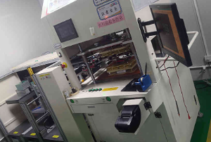
3. Bed of Nails Testing Explained
The Bed of Nails method is one of the oldest and most established electrical testing techniques for PCBs. It involves a custom-designed fixture composed of hundreds or thousands of spring-loaded pins — the “nails” — arranged precisely to contact test points on the PCB simultaneously.
How Bed of Nails Testing Works
-
Fixture Design: A custom fixture is created for each PCB design. It contains pins aligned exactly with designated test pads on the PCB.
-
Board Placement: The PCB is pressed onto the fixture so that each pin makes contact with its corresponding test point.
-
Signal Application: Electrical test signals are applied through the pins to check connectivity, shorts, opens, and other electrical characteristics.
-
Measurement: Responses are measured and compared against expected results to identify defects.
Strengths of Bed of Nails Testing
-
Speed: Because many test points are contacted simultaneously, test time per board is extremely fast — often seconds.
-
Coverage: High coverage of nets and electrical paths is possible, especially if test points are well designed.
-
Repeatability: The mechanical fixture ensures consistent, reliable contact with test points.
Limitations and Challenges
-
Fixture Cost: The upfront cost and time to design and build the fixture can be high, often thousands of dollars, and take several weeks.
-
Inflexibility: Each new PCB design requires a new fixture, which limits adaptability for prototype or small batch testing.
-
Board Damage Risk: The mechanical pressure can damage delicate or flexible PCBs.
-
Space and Maintenance: Fixtures can be bulky, requiring storage space and regular upkeep.
Despite these challenges, Bed of Nails testing remains the gold standard in high-volume PCB manufacturing due to its speed and coverage advantages.
4. Flying Probe Testing Explained
In contrast, Flying Probe testing relies on a smaller number of movable probes that travel or “fly” across the PCB surface, sequentially contacting test points rather than simultaneously.
How Flying Probe Testing Works
-
Software Programming: The testing machine is programmed with the coordinates of the test points on the PCB.
-
Probe Movement: One or more probes physically move across the PCB, touching test points one by one.
-
Signal Application and Measurement: Electrical signals are applied and measured sequentially.
-
Data Analysis: Results are compared to expected values to detect defects.
Strengths of Flying Probe Testing
-
No Fixture Needed: Eliminates the need for expensive, custom fixtures, reducing upfront cost and lead time.
-
High Flexibility: Easily handles design changes or multiple PCB types without hardware modifications.
-
Ideal for Prototypes and Low Volumes: Rapid setup and programming make it perfect for prototypes, small batches, and R&D.
-
Gentle on Boards: Less mechanical force reduces risk of damage, beneficial for flexible or sensitive PCBs.
Limitations of Flying Probe Testing
-
Slower Throughput: Testing is sequential, making it slower than Bed of Nails, which limits volume capacity.
-
Coverage Constraints: Difficult to access very densely packed or multilayer boards fully.
-
Higher Per-Unit Cost: Due to longer test times, per-board costs can be higher for mass production.
Flying Probe testing is becoming increasingly popular in the prototyping and low-volume production markets due to its flexibility and low cost.
5. The Role of Board Testing in PCB Manufacturing
In a typical PCB factory, board testing is a key step after fabrication and before assembly or shipment. The process flow usually includes:
-
PCB fabrication → Visual inspection → Board testing → Assembly → Final testing → Shipping
The objective is to catch defects as early as possible to minimize costly rework or scrap.
Board testing helps factories:
-
Achieve higher yields by identifying defective boards.
-
Reduce returns and field failures.
-
Ensure customer satisfaction through reliable products.
6. Advantages and Disadvantages of Bed of Nails Testing in Board Testing
Advantages
High Testing Speed:
Bed of Nails fixtures simultaneously contact hundreds or thousands of test points on a PCB, allowing rapid electrical tests that often complete in seconds. This speed is crucial in high-volume production where throughput directly impacts cost and delivery times.
Comprehensive Test Coverage:
Because the fixture’s pins physically contact nearly all designed test points, Bed of Nails testing can verify a broad range of electrical characteristics, including continuity, shorts, component values, and sometimes even functional checks. This thoroughness helps ensure that nearly every net is tested.
Consistent and Repeatable Results:
The rigid mechanical fixture ensures that the test points are contacted in a uniform manner every time. This repeatability reduces test variability and improves defect detection accuracy.
Integration with Automated Systems:
Bed of Nails fixtures can be integrated with automated handling, enabling continuous testing with minimal operator intervention, further increasing efficiency.
Disadvantages
High Upfront Fixture Cost:
Each PCB design requires a custom fixture that must be carefully designed, manufactured, and calibrated. The fixture cost can range from several thousand to tens of thousands of dollars, making it economically viable mainly for high-volume production.
Inflexibility to Design Changes:
Any revision or modification to the PCB design often requires re-designing and manufacturing a new fixture, resulting in delays and additional costs. This makes Bed of Nails less suitable for prototyping or small batches.
Risk of Board Damage:
The mechanical pressure from pins pressing onto test points can cause damage, especially to delicate, flexible, or thin PCBs. Careful fixture design and board handling are necessary to mitigate this risk.
Fixture Storage and Maintenance:
Fixtures occupy physical space and require regular maintenance to ensure pins remain accurate and spring-loaded mechanisms function properly. Mishandling or wear can reduce test accuracy.
7. Advantages and Disadvantages of Flying Probe Testing in Board Testing
Advantages
No Need for Custom Fixtures:
Flying Probe testing eliminates the need for a fixed physical fixture. The movable probes are controlled by software to sequentially contact test points, dramatically reducing upfront costs and lead times.
High Flexibility:
Because the test program can be quickly adapted for different PCB designs, Flying Probe testing is ideal for prototypes, small batches, or products undergoing frequent design changes. One machine can test multiple different boards with little setup.
Lower Risk of Board Damage:
Probes apply minimal mechanical force and only contact one point at a time, significantly reducing the chance of damaging delicate or flexible PCBs.
Suitable for Complex and Dense PCBs:
Advanced probe movement control allows testing on PCBs with complex routing or dense component placement, although access can still be limited compared to Bed of Nails.
Disadvantages
Slower Test Time:
Since probes contact test points sequentially rather than simultaneously, test times per PCB are longer. This makes Flying Probe less suitable for high-volume production lines where throughput is critical.
Lower Throughput:
The inherent slower speed reduces the number of boards that can be tested per hour compared to Bed of Nails.
Test Coverage Limitations:
Some areas of densely packed or multilayer PCBs may be inaccessible to the probes, resulting in potentially reduced test coverage compared to Bed of Nails fixtures.
Higher Per-Unit Cost for Large Volumes:
Longer test times translate into higher labor and machine operation costs per unit when volume increases.
8. How PCB Factories Implement Board Testing
In real-world PCB manufacturing, factories tailor their testing strategy based on product volume, complexity, and customer requirements. A typical approach includes:
For High-Volume Production
Factories prefer Bed of Nails testing for mature designs in large quantities because the high initial fixture cost is amortized over thousands or millions of units. The rapid test speed and high coverage ensure efficient quality assurance. Large factories like SQ PCB have dedicated test engineering teams to design and maintain these fixtures, integrate them with automated testers, and collect extensive test data for yield analysis.
For Prototypes and Small Volumes
For prototype runs or low-volume products, Flying Probe testing is favored due to its flexibility and low setup costs. Factories like SQ PCB can program Flying Probe machines quickly to handle new designs, making it ideal for R&D or pre-production validation.
Hybrid Approaches
Some factories employ a hybrid strategy, using Flying Probe testing during the early prototype phase and switching to Bed of Nails as volumes increase. This balances cost and speed optimally.
Data and Defect Management
Modern PCB factories integrate board testing with data collection systems that log test results, track defect trends, and facilitate rapid root cause analysis. This feedback loop helps improve yield and reduce manufacturing defects over time.
9. Recommendations for PCB Manufacturers: SQ PCB Case Study
When selecting a PCB manufacturer, partnering with a supplier experienced in various board testing methods is crucial. SQ PCB is an excellent example of a manufacturer that balances quality, flexibility, and cost through:
-
Expertise in Both Bed of Nails and Flying Probe Testing: SQ PCB’s advanced test engineering capabilities allow them to recommend and implement the best testing strategy based on customer needs.
-
Fast Turnaround for Prototypes: Utilizing Flying Probe testing, SQ PCB ensures rapid prototype validation, enabling customers to accelerate their design cycles.
-
Scalable Production: For large-volume orders, SQ PCB invests in Bed of Nails fixtures to deliver efficient and thorough testing, ensuring high-quality PCBs.
-
Comprehensive Test Coverage: SQ PCB focuses on maximizing test coverage regardless of the method to reduce defects.
-
Quality Certifications and Data Transparency: SQ PCB provides detailed test reports, ensuring customers have confidence in board quality.
By leveraging SQ PCB’s expertise, customers can enjoy streamlined board testing processes that minimize risk, cost, and lead time.
Conclusion
In the complex and fast-evolving world of PCB manufacturing, board testing stands as a critical pillar ensuring product quality, reliability, and customer satisfaction. The two primary methods — Bed of Nails and Flying Probe testing — each possess distinct strengths and weaknesses that suit different manufacturing scenarios.
Bed of Nails testing excels in high-volume production with its rapid throughput and comprehensive test coverage, albeit at the cost of high upfront fixture expenses and lower flexibility. This method remains the go-to for mature designs where economies of scale justify the investment.
Conversely, Flying Probe testing offers unmatched flexibility, minimal upfront costs, and is gentler on delicate or complex PCBs. It is especially advantageous for prototypes, small production runs, and designs undergoing frequent changes. The trade-off is slower test speeds and potentially lower coverage on very dense boards.
FAQ Section on Board Testing and Related PCB Materials
Q1: What is the difference between rolled copper foil and electrolytic copper foil?
Rolled copper foil is produced by mechanically rolling copper into thin sheets, resulting in excellent surface finish and mechanical strength. It tends to have higher tensile strength and is preferred for rigid, high-performance PCBs. Electrolytic copper foil is produced by electrodeposition and tends to be thinner, more flexible, and more cost-effective, commonly used in flexible PCBs.
Q2: How does Board Testing impact PCB reliability?
Board testing identifies defects such as shorts, opens, and incorrect component placements early in the manufacturing process. Catching these issues before assembly or shipment reduces field failures and improves overall product reliability.
Q3: Can Flying Probe testing detect all faults on a PCB?
While Flying Probe testing is versatile, it may have limitations on very dense or multilayer PCBs due to physical access restrictions. In such cases, Bed of Nails testing or combined methods may be necessary.
Q4: How long does it take to produce a Bed of Nails fixture?
Depending on complexity, fixture design and manufacturing can take from 2 to 6 weeks, which adds lead time to the production process.
Q5: Is it possible to combine Bed of Nails and Flying Probe testing?
Yes. Many manufacturers use Flying Probe testing for prototyping and troubleshooting, then transition to Bed of Nails testing for volume production, optimizing cost and efficiency.

- long board pcb
- Flexible PCBs
- Special PCB
- Express Printed Circuit Board
- Pcb Prototype
- LED PCB
- PCB
- Printed Circuit Board
- Pcb meaning
- Pcb manufacturer
- Rigid pcb board
- Rigid Flex PCB
 Quote
Quote
 E-mail