Introduction to the Finished PCB Board
A Finished PCB Board (Printed Circuit Board) is the ultimate product after completing the series of complex manufacturing and testing stages in PCB fabrication. Unlike a bare board that lacks electronic components, the finished version is fully assembled, ready for integration into electronic systems.
The board acts as a foundational platform, enabling the integration and interconnection of various electronic components. It supports both electrical conductivity and mechanical stability. Within the context of electronic equipment, the finished board is the crucial link that ensures all components communicate efficiently, perform their designated roles, and maintain overall system integrity.
The design of a Finished PCB Board considers electrical routing, thermal management, electromagnetic compatibility, and mechanical durability. From mobile devices to industrial automation controllers, these boards are indispensable in modern technology.
In this article, we’ll comprehensively explore the functions of the finished PCB board in electronic equipment, highlighting its role in electrical transmission, system architecture, thermal management, safety assurance, and more.
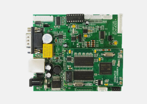
Finished PCB Board
Structural Composition of the Finished PCB Board
The Finished PCB Board typically comprises the following major layers and components:
-
Substrate Layer – The insulating base, usually made of FR-4 (fiberglass epoxy), polyimide, or metal core for specific heat dissipation needs.
-
Copper Layer – Serves as the electrical pathway. Single-sided, double-sided, or multilayer boards may contain one or more copper layers.
-
Solder Mask Layer – Prevents oxidation and prevents solder bridges.
-
Silkscreen Layer – Used for labeling component locations, part numbers, and logos.
-
Surface Finish – Coatings like HASL, ENIG, or Immersion Silver are applied to the exposed copper to ensure solderability and protection.
-
Mounted Components – The final assembly includes ICs, capacitors, resistors, transistors, and connectors.
A Finished PCB Board can be rigid, flexible, or a hybrid (rigid-flex) depending on the application, each offering different performance characteristics.
Electrical Signal Routing in Finished PCB Board
One of the primary functions of the Finished PCB Board is electrical interconnection. These signal pathways are meticulously designed to:
-
Enable uninterrupted communication between integrated components.
-
Ensure proper impedance matching for high-frequency signals.
-
Avoid cross-talk and electromagnetic interference (EMI).
-
Provide isolated grounds for analog and digital circuitry.
Advanced multilayer PCBs offer superior signal integrity due to dedicated power and ground planes. In high-speed electronics, this function is critical to maintaining signal clarity and reducing latency.
Mechanical Support Role of Finished PCB Board in Electronic Equipment
In addition to electrical functions, the Finished PCB Board provides structural and mechanical support. It holds all electronic components in place, with specific mounting holes and fixtures that align with the overall mechanical design of the device.
Mechanical properties such as vibration resistance, shock tolerance, and thermal expansion matching are essential in automotive or aerospace applications. Boards are often designed with reinforcement elements and stiffeners to ensure long-term reliability.
Thermal Management in Finished PCB Board within Electronic Equipment
Modern electronic devices generate significant heat, especially high-performance processors and power modules. A vital function of the Finished PCB Board is dissipating this heat.
Design elements that support this function include:
-
Thermal vias that transfer heat from surface to internal layers.
-
Metal core substrates (like aluminum or copper).
-
Heat sinks or spreaders mounted on high-power areas.
-
Thermally conductive dielectric materials.
If thermal management is overlooked, it could lead to circuit instability or permanent failure.
Power Distribution via Finished PCB Board in Electronic Equipment
Beyond signal routing, the Finished PCB Board efficiently distributes power from the main supply to all components. Power planes, voltage rails, and decoupling capacitors are strategically placed to:
-
Prevent voltage drops.
-
Reduce ripple.
-
Ensure uniform power delivery.
-
Filter noise and protect sensitive ICs.
In some critical systems like medical electronics or aviation-grade equipment, redundancy in power routing is included to ensure fail-safe performance.
Finished PCB Board and System Integration
The Finished PCB Board acts as the interface layer between software logic and hardware behavior. It connects sensors, actuators, displays, and user inputs to embedded control systems.
Whether it’s a simple control panel or a high-end AI-enabled robot, the Finished PCB Board ensures that hardware and software are seamlessly integrated, forming a responsive and intelligent electronic system.
For reliable system-level integration, many engineers choose trusted suppliers like SQ PCB, which offer design for manufacturability (DFM) services and testing at the final output stage.
Finished PCB Board as a Safety Barrier in Electronic Equipment
Safety compliance is a hidden but critical function of the Finished PCB Board. It integrates elements such as:
-
Fuses and protection diodes.
-
Isolation barriers for high-voltage circuits.
-
Shielding and grounding layers for EMI control.
-
Controlled creepage and clearance paths.
PCBs that fail to incorporate these safety features can be hazardous, especially in medical and industrial environments.
Using experienced manufacturers like SQ PCB ensures your boards meet UL, CE, and IPC safety standards, with integrated features right from the layout stage.
Finished PCB Board in Communication Systems of Electronic Equipment
Communication is a core requirement in modern electronic systems. The Finished PCB Board facilitates both internal and external communication channels through the integration of signal buses, data interfaces, antennas, and transceivers. Whether the communication standard is wired (e.g., USB, Ethernet, CAN bus) or wireless (e.g., Wi-Fi, Bluetooth, Zigbee), the PCB layout must support signal fidelity and noise immunity.
Designers utilize differential pairs, impedance-controlled traces, and shielding techniques on the Finished PCB Board to ensure that signals maintain integrity across varying environments. For example, in a smartphone, the PCB enables rapid switching between LTE, Wi-Fi, and Bluetooth frequencies without mutual interference.
Moreover, boards designed by manufacturers like SQ PCB often include built-in test pads and communication test features that facilitate debugging and ensure robust performance in field conditions.
Finished PCB Board Enabling Modular Design in Electronic Equipment
Another evolving function of the Finished PCB Board is to support modular design architectures. In a modular system, multiple PCBs can be interconnected via backplanes or connectors, allowing easy upgrades, maintenance, or expansion.
This modularity is common in:
-
Industrial automation controllers
-
Telecommunication racks
-
Medical diagnostic equipment
-
Automotive infotainment systems
Here, the Finished PCB Board not only carries its own components but is designed with interfaces that align with adjacent modules. This allows the system to evolve without full replacement—reducing waste and cost.
Finished-PCB Board and Embedded Intelligence in Electronic Equipment
As electronic devices become smarter, the Finished PCB Board plays a central role in embedding processing intelligence. Boards increasingly integrate microcontrollers (MCUs), digital signal processors (DSPs), memory modules, and programmable logic.
A single Finished PCB Board in a modern washing machine might include:
-
An MCU to manage cycle logic.
-
An EEPROM to store usage data.
-
A Bluetooth module for app-based control.
-
Sensor interfaces to measure water levels, vibration, and temperature.
This embedded intelligence turns passive electronics into adaptive systems capable of learning, communicating, and optimizing their operation in real time.
Finished-PCB Board’s Role in Environmental Durability of Electronic Equipment
Electronic equipment often operates in diverse and sometimes harsh environments, such as automotive engine compartments, industrial plants, or outdoor communication devices. The Finished PCB Board must ensure operational reliability under varying temperatures, humidity, vibration, and chemical exposure.
Key design and manufacturing considerations include:
-
Conformal Coating and Potting: Protective layers applied to the Finished PCB Board to shield against moisture, dust, and corrosive substances.
-
Material Selection: Use of high-Tg (glass transition temperature) substrates, flexible materials for vibration resistance, and metal-core boards for heat dissipation.
-
Thermal Cycling Resistance: The board and components must endure repeated heating and cooling without mechanical failure.
-
Mechanical Reinforcement: Additional stiffeners and support structures may be incorporated for boards subject to shock and vibration.
In such demanding conditions, partnering with experienced PCB suppliers like SQ PCB ensures that the Finished PCB Board meets stringent durability standards required for mission-critical electronics.
Finished-PCB Board in Custom and Emerging Applications
The rapid evolution of technology drives new applications where the Finished PCB Board assumes specialized functions:
-
Wearable Electronics: Ultra-thin, flexible Finished PCB Boards conform to curved surfaces and endure continuous motion.
-
IoT Devices: Boards are optimized for ultra-low power consumption and compact form factors.
-
Automotive Advanced Driver-Assistance Systems (ADAS): High-reliability multilayer Finished PCB Boards with embedded sensors and safety features.
-
Aerospace and Defense: Rigid-flex boards with high-temperature and radiation resistance.
These customized PCB solutions often require novel materials, microvia technologies, and advanced surface finishes, underscoring the importance of choosing suppliers with strong R&D capabilities such as SQ PCB.
Advanced Functionalities of the Finished-PCB Board
Beyond basic interconnection, modern Finished PCB Boards include additional embedded functionalities such as:
-
Embedded Passives: Resistive and capacitive elements integrated directly into the board to reduce component count and improve signal integrity.
-
Shielding Layers: Embedded metal layers to protect sensitive circuitry from EMI.
-
High-Density Interconnects (HDI): Microvias and blind/buried vias enable complex routing in miniature spaces.
-
Built-In Self-Test (BIST) Features: Integrated test circuits that allow the device to self-diagnose during operation.
These enhancements improve performance, reliability, and maintainability of the electronic equipment.
The Relationship Between PCB Manufacturing Processes and the Finished-PCB Board Functionality
The quality and capabilities of a Finished PCB Board are fundamentally influenced by the manufacturing processes it undergoes. Each stage of PCB fabrication impacts the board’s performance in electronic equipment:
1. Material Selection and Lamination
The choice of substrate material (e.g., FR-4, polyimide, metal core) and lamination quality determine the mechanical strength, thermal endurance, and dielectric properties of the Finished PCB Board. High-quality lamination ensures layer adhesion, which is vital to maintain electrical isolation and prevent delamination during thermal cycling.
2. Etching and Copper Patterning
Precision in etching controls the accuracy of copper traces and pads, directly affecting signal integrity and current-carrying capacity. Uneven etching or over-etching can cause open circuits or short circuits, compromising the Finished PCB Board’s function.
3. Drilling and Via Formation
Microvias, blind vias, and through-holes provide electrical connections between layers. Proper drilling accuracy and plating ensure low-resistance paths and mechanical robustness. Defects here often lead to PCB open circuits or reliability failures.
4. Surface Finishing
Finishes such as ENIG (Electroless Nickel Immersion Gold), OSP (Organic Solderability Preservative), or Immersion Tin protect exposed copper and facilitate soldering. The choice of finish influences the board’s lifespan, solder joint reliability, and environmental resistance.
5. Solder Mask and Silkscreen Printing
Solder masks prevent unintended solder bridges and protect circuits from environmental damage. Silkscreens provide essential assembly and maintenance information. Their accuracy supports manufacturing consistency and reduces assembly errors.
6. Assembly and Soldering
Component placement precision and soldering quality are crucial. Modern surface-mount technology (SMT) and automated optical inspection (AOI) systems contribute to consistent, defect-free Finished PCB Boards.
The interaction between these manufacturing processes and material choices culminates in the overall performance and durability of the Finished PCB Board within electronic equipment. Therefore, partnering with manufacturers like SQ PCB, who control and optimize these steps, is critical to ensuring superior Finished PCB Board functionality.
The Role of Finished-PCB Board in Power Efficiency of Electronic Equipment
Power efficiency is a critical design goal for modern electronic equipment, from battery-powered wearables to large data centers. The Finished PCB Board contributes by:
-
Minimizing Resistive Losses: Using thicker copper layers or wider traces reduces resistance, lowering power dissipation.
-
Optimizing Power Plane Design: Dedicated power and ground planes minimize noise and improve current distribution.
-
Incorporating Power Management ICs (PMICs): Placing PMICs and associated components on the Finished PCB Board enhances voltage regulation and battery life.
-
Thermal Management: Efficient heat dissipation prevents power loss and prolongs component life.
Effective power management on the Finished PCB Board translates directly to longer battery life, less heat generation, and improved overall device performance.
Finished-PCB Board in High-Speed Digital and RF Applications
High-speed digital and radio frequency (RF) applications impose stringent requirements on the Finished PCB Board:
-
Controlled Impedance Traces: Precise control over trace width, spacing, and dielectric constants to maintain signal integrity.
-
Layer Stack-Up Optimization: Arranging layers to minimize crosstalk and EMI.
-
Use of Low-Loss Materials: To reduce signal attenuation at high frequencies.
-
Shielding and Grounding Techniques: To isolate sensitive circuits and reduce noise.
Such design sophistication ensures that Finished PCB Boards in networking equipment, 5G devices, and radar systems perform reliably at GHz frequencies.
Summary
The Finished PCB Board serves as the fundamental platform for electronic equipment, providing electrical connectivity, mechanical support, thermal management, power distribution, system integration, and safety assurance. Its design and manufacturing quality directly influence device performance, reliability, and user experience.
Leading PCB manufacturers, SQ PCB play a pivotal role by delivering high-quality Finished PCB Boards tailored for diverse applications — from consumer electronics to aerospace — with ongoing innovation and adherence to industry standards.
FAQs about Finished PCB Board and PCB Materials
1. What is the difference between rolled copper foil and electrolytic copper foil?
Rolled copper foil is mechanically pressed, offering superior surface uniformity and mechanical strength, making it ideal for flexible PCBs and high-reliability applications.
Electrolytic copper foil is formed through electrochemical deposition and is more cost-effective and flexible but less robust than rolled foil.
2. How does a Finished PCB Board differ from a bare PCB?
A Finished PCB Board includes mounted components and is fully tested, ready for integration. In contrast, a bare PCB is the etched board without any soldered parts.
3. Can a Finished PCB Board handle high-frequency signals?
Yes, depending on the dielectric materials used, trace width, and design layout. Boards meant for RF or microwave use often include controlled impedance and low-loss materials.
4. What testing methods are used for Finished PCB Boards?
Common tests include ICT (In-Circuit Testing), flying probe testing, functional tests, and X-ray inspection, ensuring functionality and detecting soldering or component defects.
5. Is it better to use multilayer Finished PCB Boards for complex devices?
Absolutely. Multilayer PCBs provide greater routing flexibility, reduce electromagnetic interference, and improve performance in complex, high-speed or compact electronic devices.

- long board pcb
- Flexible PCBs
- Special PCB
- Express Printed Circuit Board
- Pcb Prototype
- LED PCB
- PCB
- Printed Circuit Board
- Pcb meaning
- Pcb manufacturer
- Rigid pcb board
- Rigid Flex PCB
 Quote
Quote
 E-mail