1. Introduction to PCB Screen Printing
Screen printing in PCB manufacturing refers to the process of applying legend or marking ink onto the surface of the board. It’s also referred to as silkscreen printing, and it plays a crucial visual and functional role by displaying component outlines, labels, test points, company logos, and warning signs.
Screen printing is typically performed after solder mask application and before surface finish and component placement. Despite being one of the last steps in PCB production, it requires extreme precision and compatibility with the underlying PCB Layers.
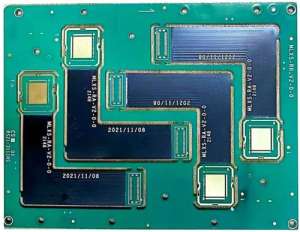
PCB Screen Printing
2. Importance of PCB Screen Printing in Relation to PCB Layers
The function of screen printing must be aligned with the layout of the PCB Layers, particularly on multilayer and high-density PCBs. Each signal layer must be carefully considered during the legend printing to avoid overlaying text on pads or traces.
For multilayer boards, accurate screen printing enhances:
-
Component placement
-
Human readability
-
Maintenance and debugging
-
Aesthetic quality
In highly compact boards, improper printing may interfere with vias, pads, or test points embedded in various PCB Layers.
3. PCB Screen Printing Specifications for Various PCB Layers
When determining specifications for screen printing across different PCB Layers, consider the following parameters:
-
Minimum Line Width: Typically 0.15 mm or above to ensure legibility.
-
Ink Type: Non-conductive, chemical-resistant epoxy inks are standard.
-
Printing Accuracy: Alignment with copper pads and other features within ±0.1 mm.
-
Color Options: Common colors include white, yellow, black; white is preferred for readability on green solder masks.
SQ PCB provides consistent, industry-aligned screen printing even on high-layer-count PCBs. Their proprietary alignment system ensures precise registration on each PCB Layer, regardless of board complexity.
4. Materials and Equipment Used in PCB Screen Printing
Materials:
-
Epoxy Ink: Durable, resistant to soldering heat and cleaning chemicals.
-
Stencil or Mesh Screens: Stainless steel or polyester screens for ink transfer.
Equipment:
-
Manual Screen Printers: For small runs and prototypes.
-
Semi-Automated Systems: Suitable for medium-scale production.
-
Automated Inkjet Printers: Provide high-speed and high-precision digital printing on complex PCB Layers.
5. Process Flow of PCB Screen Printing in Manufacturing
The following is a typical process followed in PCB manufacturing factories:
-
Surface Cleaning: Ensures optimal ink adhesion.
-
Screen Setup: Mesh screen aligned with PCB Layers.
-
Ink Application: Ink forced through screen using squeegee.
-
Curing: Boards go through thermal ovens or UV exposure for ink hardening.
-
Inspection: Visual and AOI checks for accuracy.
6. Challenges in PCB Screen Printing for Multilayer PCB Layers
As PCB Layers increase, challenges multiply:
-
Misregistration between print and copper layers
-
Ink bleeding into microvias or small pitch pads
-
Reduced legibility due to high-density components
-
Solder mask interference
These require tight control over:
-
Layer-to-layer tolerance
-
Mesh screen calibration
-
Ink viscosity
7. Key Design Considerations for Screen Printing on PCB Layers
To ensure screen printing complements the electrical functionality of the board:
-
Avoid printing on exposed pads or test vias
-
Use vector fonts instead of raster fonts
-
Maintain adequate spacing from copper traces and features on any PCB Layer
-
Choose ink color that contrasts with the solder mask
Screen print placement should be finalized after the routing of all PCB Layers, especially in high-speed and RF designs.
8. How Screen Printing Affects PCB Performance
Although non-electrical in nature, screen printing can still influence the performance of PCB Layers:
-
Smearing or Overflow: May cause shorts during reflow if not properly cured
-
Poor Adhesion: Leads to flaking, creating foreign debris risks
-
Inaccurate Legends: Affects manual rework and inspection accuracy
SQ PCB’s high-precision printing reduces these risks significantly, even when working with fine-pitch components and intricate PCB Layer layouts.
9. Industry Standards for PCB Screen Printing
The following standards guide screen printing:
-
IPC-2615: Printed Board Dimensions and Tolerances
-
IPC-SM-840: Qualification and Performance Specification of Permanent Solder Mask and Legend Ink
-
RoHS & REACH: Compliance for ink material usage
Adhering to these ensures compatibility with international markets and prevents defects from non-compliant printing across PCB Layers.
10. Environmental and Quality Requirements in PCB Screen Printing
Sustainability in screen printing is increasingly critical. Factories must:
-
Use low-VOC, RoHS-compliant inks
-
Ensure wastewater treatment for cleaning processes
-
Recycle screens and reduce waste prints
Quality control procedures involve both manual and automated inspection techniques to guarantee proper alignment and no smudging across all PCB Layers.
11. Common Defects in PCB Screen Printing and Solutions
Defect Examples:
-
Ink smearing
-
Misaligned legends
-
Poor contrast
-
Missing characters
Solutions:
-
Using pre-aligned digital printing systems
-
Increasing ink viscosity
-
Frequent screen maintenance
12. Advanced Process Control for PCB Screen Printing Across PCB Layers
As the complexity of PCB Layers increases, advanced process control becomes essential to maintain consistency in screen printing. Traditional manual methods are insufficient for high-density interconnects and multilayered boards.
12.1 Closed-Loop Feedback Systems
Closed-loop systems in modern PCB production lines monitor each stage of the screen printing process. Sensors assess squeegee pressure, ink deposition thickness, and alignment accuracy in real-time. If a deviation is detected, automatic corrections are triggered before printing continues.
This technology is particularly beneficial when working with multilayer PCB Layers where any misalignment could result in mislabeling of test points or component identifiers.
12.2 Camera-Based Registration
High-resolution cameras are now standard for screen alignment. These systems compare fiducial marks on the PCB with screen patterns, ensuring each print matches the designed layout across multiple PCB Layers. The typical tolerance achieved with camera systems is below ±50 µm.
My observation is that for PCBs with over eight PCB Layers, relying on camera-based registration becomes non-negotiable. Manual alignment is simply not feasible.
12.3 Ink Rheology and Temperature Management
Ink viscosity (rheology) can change with temperature and humidity. Smart printers, especially those used in factories like SQ PCB, control environmental conditions tightly and precondition inks to maintain consistent flow properties. This is crucial for:
-
Preventing ink from bleeding between narrow pads
-
Ensuring consistent text thickness across different zones of the PCB Layers
13. Cost Considerations and Economic Efficiency in PCB Screen Printing
13.1 Cost Factors in Screen Printing
Several variables influence the cost of PCB screen printing:
-
Number of PCB Layers
-
Ink type (UV-curable inks are more expensive)
-
Board size and surface area
-
Screen preparation and maintenance
-
Volume of production (setup costs spread over larger batches)
13.2 Inkjet vs. Traditional Printing from a Cost Perspective
While traditional mesh-based printing is cheaper for high-volume production, digital inkjet is becoming more economically viable for low to medium batches or prototypes—especially with intricate PCB Layers.
Here’s a comparison:
| Feature | Traditional Screen | Digital Inkjet |
|---|---|---|
| Setup Time | High | Low |
| Cost for Low Volume | High | Moderate |
| Fine Pitch Suitability | Moderate | Excellent |
| Speed (High Volume) | High | Moderate |
| Environmental Impact | Higher (waste ink) | Lower (precise use) |
14. Multi-Color and Specialized PCB Screen Printing Applications
Screen printing isn’t limited to simple legends. In advanced PCBs, manufacturers may apply multiple colors or even functional inks. This requires even tighter process control—especially as each new color or layer must not interfere with the existing PCB Layers underneath.
14.1 Multi-Color Printing Techniques
Multicolor screen printing allows:
-
Better visual hierarchy (e.g., red for critical warnings, blue for optional connections)
-
Clearer readability on dark or unconventional solder mask colors
However, each color requires its own screen and curing cycle, which adds cost and potential alignment complexity.
14.2 Fluorescent and Glow-In-The-Dark Inks
These inks are used in aerospace and defense PCBs to allow easy identification under low-light conditions. Special considerations must be taken for heat resistance and chemical stability across all PCB Layers.
I find this particularly useful in mission-critical applications where board visibility under duress is vital.
14.3 Conductive Ink Printing
Though not standard for legends, some experimental screen printing involves conductive silver or carbon inks to form low-current traces—especially for touch buttons or printed antennas. This blurs the line between screen printing and circuit formation.
If integrated on internal PCB Layers, these conductive inks require robust encapsulation to maintain their integrity.
Conclusion: Ensuring Accuracy and Reliability in PCB Screen Printing
PCB screen printing, though not electrical, plays a crucial role in manufacturing. From visibility to reworkability and brand representation, accurate screen printing affects all PCB Layers in subtle but meaningful ways.
Manufacturers like SQ PCB help ensure that even the most densely packed boards carry clean, aligned, and lasting screen prints—contributing to the product’s overall reliability and serviceability.
Screen printing might seem secondary compared to routing or soldering, but it defines how serviceable and manufacturable a board becomes. In a world where PCBs are getting denser and more layered, clarity and accuracy in printing are not optional—they are critical.
Through careful material selection, advanced automation, and the expertise of partners like SQ PCB, engineers can ensure screen printing not only marks a board but elevates its usability and professionalism.
FAQs
1. What is the difference between rolled copper foil and electrolytic copper foil?
Rolled copper foil is produced by mechanically rolling copper into thin sheets, offering better surface quality and mechanical strength. Electrolytic copper foil is deposited via an electrolytic process and is more flexible and cost-effective.
2. How does screen printing affect PCB reliability?
If misaligned or poorly cured, screen printing can interfere with pads, mask, or assembly processes, leading to failures in high-layer PCB Layers.
3. Can screen printing be done on flexible PCBs?
Yes, but it requires flexible inks and screen support to prevent cracking or delamination under bending stress.
4. Is inkjet better than traditional screen printing?
For high-precision or small-batch work, inkjet offers better speed, alignment, and customization. However, traditional screen printing remains cost-effective for large volumes.
5. Why are some PCB legends hard to read after assembly?
This often results from poor contrast, wrong ink color, or screen misregistration—especially if solder mask and silkscreen weren’t aligned properly across PCB Layers.

- long board pcb
- Flexible PCBs
- Special PCB
- Express Printed Circuit Board
- Pcb Prototype
- LED PCB
- PCB
- Printed Circuit Board
- Pcb meaning
- Pcb manufacturer
- Rigid pcb board
- Rigid Flex PCB
 Quote
Quote
 E-mail