1. Understanding Welding Double-Sided Circuit Boards
Welding Double-Sided Circuit Boards involves soldering components on both the top and bottom layers of a PCB. Unlike single-sided boards, these utilize conductive copper layers on both surfaces, allowing for a higher component density and more complex circuit configurations.
This type of board enables intricate routing options. Traces can cross over each other via plated through-holes (vias), and components can be strategically placed to optimize performance. In manufacturing, the process requires precise coordination between Surface Mount Technology (SMT) and Through-Hole Technology (THT).
Key Concepts:
-
Double-sided PCB: A board with copper tracks on both sides.
-
Via: Small plated holes that connect traces from one side to the other.
-
SMT vs THT: SMT components are soldered directly onto the surface, while THT components are inserted into holes and soldered on the opposite side.
Historical Context and Industry Evolution
In the early days of electronics, single-sided PCBs dominated because of their simplicity and ease of manufacturing. However, as electronics became more sophisticated—especially in telecommunications, automotive, and consumer gadgets—designers faced the challenge of fitting more circuits into limited space. Double-sided PCBs emerged as a natural evolution to address this challenge, allowing components and traces on both sides, which effectively doubled the available area for circuitry without significantly increasing board size.
The welding process had to evolve accordingly. Early manual soldering methods gave way to automated techniques like wave soldering and reflow soldering, capable of handling the increased complexity of double-sided assembly with higher precision and throughput.
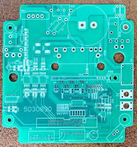
Welding double-sided circuit boards
2. Pros and Cons of Welding Double-Sided Circuit Boards
Advantages of Welding Double-Sided Circuit Boards
-
Compact Design
The use of both sides of the board enables the design of smaller devices without sacrificing circuit complexity. -
Enhanced Electrical Performance
Shorter traces and better signal integrity are possible due to improved layout options. -
Higher Component Density
Ideal for advanced applications like IoT, automotive electronics, and industrial controllers. -
Cost-effective for Mid-Complex Projects
Less expensive than multilayer PCBs, yet more capable than single-sided boards. -
Improved Thermal Management
Components can be distributed across both surfaces, reducing localized heat buildup.
Disadvantages of Welding Double-Sided Circuit Boards
-
More Complex Manufacturing
Aligning and soldering on both sides requires precision, increasing the risk of soldering defects. -
Time-Consuming Assembly
Double pass soldering processes (top and bottom) require more time and oversight. -
Difficult Repair and Inspection
Fault diagnosis becomes challenging when components are located on both surfaces. -
Limited for Very High-Speed Circuits
They may not always meet the demands of ultra-high-frequency signal integrity, unlike multilayer PCBs.
3. Key Considerations When Welding Double-Sided Circuit Boards
Importance of Welding Double-Sided PCBs
Welding double-sided PCBs is crucial for creating compact and reliable electronic assemblies. It enables designers to:
-
Maximize board real estate without increasing size or cost significantly
-
Achieve more intricate electrical routing and multi-functional circuits
-
Balance component placement to optimize thermal dissipation and mechanical strength
However, welding double-sided PCBs demands careful control of soldering parameters, alignment, and inspection, since the dual-sided nature introduces challenges such as heat management, warping, and defect inspection complexity.
To ensure high-quality results, consider the following:
1. Component Placement Strategy
The way components are placed on both sides affects not only soldering quality but also thermal management and mechanical strength.
-
Balanced Distribution: Placing high-heat components on opposite sides helps to prevent localized overheating. For example, power regulators might be placed on the top while smaller ICs are on the bottom.
-
Accessibility: Components that may require future rework or testing should be positioned where access is easiest.
-
Avoid Overlapping Components: Overlapping components on opposite sides can complicate soldering and increase risk of damage during assembly.
-
Mechanical Stability: Heavy or stress-prone components (like connectors) should be placed where the PCB has additional mechanical support, often on one side.
2. Soldering Sequence and Process Control
-
Bottom Side First: Usually, the bottom side is soldered first—often SMT components via reflow soldering. This prevents heat from the second soldering process from damaging components already soldered.
-
Top Side Second: The top side components, often through-hole, are soldered afterward, either by wave soldering, selective soldering, or manual soldering.
-
Thermal Profile Design: Each soldering process must have a thermal profile tailored to the components and board materials, to avoid overheating or insufficient soldering.
3. Thermal Management and Warpage Prevention
-
Symmetrical Copper Distribution: Uneven copper on one side can cause warping during soldering due to different thermal expansion rates. Designers should aim for symmetry where possible.
-
Use of Reinforcements: Stiffeners or heat sinks can be added to minimize bending.
-
Thermal Simulation: Advanced software tools can predict thermal stresses and warpage, enabling proactive design adjustments.
4. Solder Mask and Surface Finish Alignment
-
Precision Solder Mask Registration: Misalignment leads to solder bridging or open circuits. High-precision lithography is necessary.
-
Surface Finish Choice: The choice between HASL, ENIG, or lead-free HASL affects solderability and long-term reliability.
5. Quality Control and Testing
-
Automated Optical Inspection (AOI): Essential after both soldering steps to detect solder bridges, insufficient solder, and misaligned components.
-
X-Ray Inspection: Particularly useful for through-hole joints and hidden solder areas.
-
Electrical Testing: Functional and in-circuit testing ensures all connections work as designed.
-
Environmental Stress Testing: Thermal cycling and vibration tests verify robustness.
4. Common Soldering Challenges in Welding Double-Sided Circuit Boards
4.1 Warping During Reflow
Improper temperature profiles can cause PCB warpage, especially when one side has more copper than the other.
4.2 Solder Bridges
Bridging between closely spaced pads is common, especially on fine-pitch ICs. Stencil design and printing pressure must be controlled.
4.3 Tombstoning of Components
This SMT defect occurs when uneven heating lifts one side of a component off the pad. Symmetrical pad design can help mitigate this.
4.4 Through-Hole Pin Obstruction
Bottom-side SMT components may interfere with wave soldering of THT pins. Proper clearance should be designed.
5. Why Choose SQ PCB for Welding Double-Sided Circuit Boards?
SQ PCB has earned a reputation for delivering high-quality double-sided boards with precision manufacturing and fast turnaround times. Their advanced equipment ensures tight solder mask tolerances and effective reflow/wave soldering profiles.
Their engineering support helps customers select suitable pad designs, via configurations, and materials for effective double-sided assembly.
6. Material Selection for Welding Double-Sided Circuit Boards
Selecting the appropriate materials is foundational to achieving high-quality, reliable double-sided circuit boards. Materials affect not only the soldering process but also electrical performance, mechanical strength, and thermal management.
1. Copper Foil
Copper foil forms the conductive traces on both sides of the PCB. The choice of copper foil type influences solderability, flexibility, and overall board durability.
-
Rolled Copper Foil
Rolled copper foil is produced by mechanically rolling copper into thin sheets. This process aligns the grain structure, resulting in a smoother surface and greater mechanical strength. Rolled foil provides excellent adhesion to the substrate and reduces the likelihood of cracking during bending or thermal cycling. It is especially beneficial for high-reliability applications where mechanical stress is a concern. -
Electrolytic Copper Foil
Electrolytic copper foil is produced by electroplating copper onto a rotating drum. It is more flexible and cost-effective than rolled foil but has a rougher surface texture. The increased surface roughness can improve adhesion of the copper to the substrate but may result in higher signal losses at very high frequencies. Electrolytic foil is widely used in standard applications where cost efficiency is critical.
2. Base Substrate Material
The substrate forms the structural foundation of the PCB. Its thermal, mechanical, and electrical properties are essential considerations.
-
FR4
FR4 is the most common substrate material, composed of woven fiberglass reinforced with epoxy resin. It offers good mechanical strength, electrical insulation, and moisture resistance, suitable for most general-purpose double-sided PCBs. -
High Tg FR4
For applications requiring higher thermal resistance, such as automotive or industrial electronics, high glass transition temperature (Tg) FR4 substrates are preferred. They withstand higher reflow temperatures without deformation. -
Ceramic or Composite Substrates
In advanced or high-frequency applications, ceramic-based or composite substrates provide superior thermal conductivity and electrical performance but at a higher cost.
3. Solder Mask Materials
The solder mask protects copper traces from oxidation and prevents solder bridges during assembly.
-
Liquid Photo-Imageable (LPI) Solder Mask
The most commonly used solder mask type, LPI provides high resolution and durability. It is suitable for fine-pitch components commonly found on double-sided PCBs. -
Dry Film Solder Mask
Offers thicker coverage and is preferred for boards subjected to harsh environments.
4. Surface Finishes
The surface finish on the exposed copper pads affects solderability and shelf life.
-
Hot Air Solder Leveling (HASL)
HASL is a cost-effective finish involving coating pads with molten solder and leveling with hot air. It provides excellent solderability but can result in uneven surfaces. -
Electroless Nickel Immersion Gold (ENIG)
ENIG offers a flat surface with excellent oxidation resistance and is preferred for fine-pitch SMT components. -
Lead-Free HASL
To meet environmental standards, lead-free HASL options are widely adopted, though they require careful thermal management during soldering.
7. Application Examples of Welding Double-Sided Circuit Boards
Double-sided circuit boards are widely used across diverse industries, serving as the backbone for countless electronic devices and systems. Their ability to offer compact, efficient, and reliable circuitry makes them indispensable in modern electronics.
1. Consumer Electronics
In devices such as smartphones, tablets, smartwatches, and digital cameras, space is at a premium. Welding double-sided PCBs allows manufacturers to integrate more components into smaller packages without sacrificing functionality.
-
Smartphones and Tablets: High-density circuitry with components like processors, memory chips, sensors, and power management ICs are mounted on both sides to maximize performance in slim designs.
-
Wearables: Smartwatches and fitness trackers rely heavily on double-sided PCBs to pack advanced sensors and communication modules into tiny form factors.
2. Automotive Electronics
The automotive industry demands high reliability and performance in challenging environments, such as temperature extremes and mechanical vibration.
-
Engine Control Units (ECUs): Double-sided PCBs are used to support complex processing and signal conditioning circuits.
-
Lighting Systems: Advanced LED drivers and control circuits benefit from the dense layout capabilities of double-sided boards.
-
Infotainment Systems: These require multi-functional PCBs capable of supporting audio, video, and connectivity features simultaneously.
3. Medical Devices
Medical electronics prioritize precision, reliability, and miniaturization.
-
Diagnostic Equipment: Devices like portable blood analyzers use double-sided PCBs to handle sensitive sensor signals alongside processing circuits.
-
Monitoring Systems: Patient monitors and wearable health devices utilize compact double-sided PCBs to integrate multiple functions within a small footprint.
4. Industrial and Automation Equipment
Industrial control systems, programmable logic controllers (PLCs), and robotics depend on robust electronic assemblies.
-
Automation Controllers: Dense circuitry on double-sided PCBs facilitates complex logic and I/O handling in compact enclosures.
-
Sensors and Actuators: Integrated control and sensing circuits benefit from the flexibility offered by double-sided layouts.
5. Telecommunications
Telecom equipment often requires high-frequency signal handling and compact, high-density PCB designs.
-
Network Routers and Switches: Double-sided PCBs provide the necessary routing density for signal processing and network interfaces.
-
Wireless Communication Devices: These use double-sided PCBs to integrate RF components and control electronics efficiently.
Conclusion
Welding double-sided circuit boards represents a vital step in the evolution of electronics manufacturing. It embodies the ongoing pursuit of higher functionality, miniaturization, and cost-efficiency that drives our industry forward.
From my perspective, mastering the nuances of this process is key to unlocking the full potential of modern PCB design. The ability to mount components on both sides of a board not only increases circuit density but also enables innovative layouts that improve electrical performance and thermal management.
However, these benefits do not come without challenges. The dual-sided nature adds complexity to soldering, inspection, and repair, demanding a deep understanding of materials, thermal profiles, and assembly techniques. Careful component placement, balanced copper distribution, and precise process control are essential to mitigate risks such as warpage, solder bridges, and heat damage.
Looking ahead, as devices continue to shrink and demands on electronics intensify, the relevance of double-sided PCB welding will only grow. Those who invest in mastering this technology position themselves to innovate effectively and deliver superior products.
In conclusion, welding double-sided circuit boards is not merely a manufacturing step—it is an enabler of modern electronics’ complexity and sophistication. Embracing its challenges with diligence, knowledge, and the right partners opens the door to endless possibilities.
1. What is the difference between rolled copper foil and electrolytic copper foil?
Rolled copper foil is produced by mechanically rolling copper into thin sheets, which aligns the grain structure and results in a smoother surface and superior mechanical strength. This makes rolled copper foil ideal for applications requiring higher durability and better adhesion to the substrate.
Electrolytic copper foil is created through an electroplating process where copper is deposited onto a drum, resulting in a rougher surface texture. It is more flexible and cost-effective but may have slightly higher electrical losses at very high frequencies. Electrolytic foil is commonly used for standard applications where cost efficiency is a priority.
2. Can both sides of a double-sided PCB have SMT components?
Yes, it is possible to mount SMT components on both sides of a double-sided PCB. However, this increases manufacturing complexity as the soldering process must be carefully sequenced to avoid damaging components previously soldered on the opposite side. Generally, the side with fewer or more sensitive components is soldered second, using controlled thermal profiles or selective soldering techniques.
3. What causes tombstoning in SMT components?
Tombstoning occurs when one end of a small SMT component lifts off the pad during soldering, giving it a “tombstone” appearance. It is typically caused by uneven wetting forces due to thermal gradients, inconsistent solder paste application, or imbalanced pad design. Proper stencil design, balanced thermal profiling, and symmetrical pad layouts help prevent tombstoning.
4. How does selective soldering differ from wave soldering?
Wave soldering involves passing the PCB over a wave of molten solder, simultaneously soldering all through-hole components on one side. It is efficient for boards with less complex or densely packed components but can risk heat damage on sensitive parts.
Selective soldering uses a controlled mini-wave or solder nozzle to target specific pins or areas on the PCB. It is ideal for densely packed or double-sided boards where only certain regions require soldering, minimizing thermal stress on other components.
5. Is rework safe for Welding Double-Sided Circuit Boards?
Rework on double-sided PCBs is possible but must be approached with caution. The thermal exposure during rework on one side can damage components or solder joints on the opposite side. Using precision rework stations with controlled heating, preheating the board, and following proper process protocols help ensure successful rework without compromising board integrity.

- long board pcb
- Flexible PCBs
- Special PCB
- Express Printed Circuit Board
- Pcb Prototype
- LED PCB
- PCB
- Printed Circuit Board
- Pcb meaning
- Pcb manufacturer
- Rigid pcb board
- Rigid Flex PCB
 Quote
Quote
 E-mail