Introduction: Understanding Circuit Board Short Circuits in PCB Manufacturing
In the intricate world of PCB (Printed Circuit Board) manufacturing, maintaining electrical integrity is paramount. One of the most pressing issues that can compromise functionality is the occurrence of Circuit Board Short Circuits. These defects not only disrupt performance but also pose serious risks to devices and users alike. This article explores what causes these shorts, how manufacturers address them, and strategies for prevention.
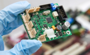
Circuit Board Short Circuits
What Are Circuit Board Short Circuits?
Circuit Board Short Circuits refer to unintended low-resistance paths between two or more conductors, allowing excessive current to flow through a part of the PCB. This often results in overheating, component damage, or complete system failure.
Causes of Circuit Board Short Circuits:
-
Solder Bridging: Excessive solder creating unintended connections between pads.
-
Foreign Conductive Materials: Dust, metal filings, or flux residue.
-
Design Flaws: Inadequate spacing in high-density layouts.
-
Layer Misalignment: In multilayer PCBs, misregistration can cause shorts.
-
Manufacturing Defects: Poor etching, over-drilling, or poor solder mask application.
Circuit Board Short Circuits and Their Impact on Final Products
The effects of Circuit Board Short Circuits can range from minor malfunctions to catastrophic system failures. In consumer electronics, this may lead to product recalls. In medical or aerospace applications, the stakes are far higher. Understanding the implications motivates manufacturers to adopt rigorous inspection and testing procedures.
Inspection Techniques for Detecting Circuit Board Short Circuits
PCB manufacturers use several techniques to identify Circuit Board Short Circuits before boards reach the customer:
-
Automated Optical Inspection (AOI): High-resolution cameras detect visual defects.
-
In-Circuit Testing (ICT): Electrical probes check for correct resistance and shorts.
-
Flying Probe Testing: Useful for low-volume, high-mix production.
-
X-ray Inspection: Detects hidden shorts in BGA and multilayer boards.
-
Boundary Scan: Applies to complex digital boards using JTAG-compatible devices.
These inspections are often carried out at multiple stages to ensure high reliability.
How PCB Manufacturers Handle Detected Circuit Board Short Circuits
When Circuit Board Short Circuits are identified during inspection or testing, manufacturers follow standardized protocols:
-
Isolation of Defective Units: Affected boards are immediately separated from the production line.
-
Root Cause Analysis: Engineers analyze production data and test logs to trace the origin of the fault.
-
Microscopic Examination: Detailed visual inspection helps pinpoint flaws like debris or solder bridges.
-
Reworking or Scrapping: Minor defects might be repaired manually; major ones are scrapped.
-
Process Adjustment: If the cause is traced to a process error (e.g., screen printing, soldering), adjustments are made.
Preventive Design Practices to Avoid Circuit Board Short Circuits
To minimize Circuit Board Short Circuits, PCB designers follow best practices:
-
Adequate Clearance: IPC-2221 standards recommend safe spacing between conductors.
-
Solder Mask Usage: High-quality masks prevent bridges and conductive contaminants.
-
Design Rule Checks (DRC): CAD tools flag spacing violations before production.
-
Proper Via Placement: Poor via layout can cause accidental connections in multilayer boards.
-
Minimized Crosstalk: Routing techniques reduce potential interference.
Early attention to layout and simulation can prevent downstream issues.
Material Selection’s Role in Circuit Board Short Circuits
The choice of materials directly affects the likelihood of Circuit Board Short Circuits:
-
High-quality copper foils: Reduce the chance of burrs and over-etching.
-
Reliable laminates: Improve insulation between conductive layers.
-
Consistent solder mask: Avoids pinholes or peeling.
✅ Professional suppliers like SQ PCB emphasize certified materials and IPC-compliant processes, helping mitigate short circuit risks.
Solder Bridging as a Major Cause of Circuit Board Short Circuits
Among the various causes of Circuit Board Short Circuits, solder bridging remains one of the most common and persistent issues in the manufacturing process. This occurs when excess solder unintentionally connects two adjacent pads or leads, creating a conductive path that wasn’t part of the original design.
In surface-mount technology (SMT) assembly lines, the solder paste is applied using a stencil. If the stencil is misaligned, or if too much paste is deposited, bridging may occur during the reflow process. Additionally, insufficient solder mask between fine-pitch components can exacerbate the chance of solder forming unintended connections.
To mitigate solder bridging:
-
Use laser-cut, stainless-steel stencils with correct aperture designs.
-
Ensure tight stencil-to-board alignment and appropriate squeegee pressure.
-
Apply solder mask dams between fine-pitch pads for critical components.
Manufacturers like SQ PCB implement stringent solder paste volume control, along with 3D solder paste inspection (SPI) systems to detect excessive deposition before boards enter reflow ovens. This significantly reduces solder bridging and thus Circuit Board Short Circuits.
Foreign Particles and Contaminants That Cause Circuit Board Short Circuits
Tiny conductive particles, such as metal shavings, dust, or flux residues, can also be responsible for Circuit Board Short Circuits, especially during or after assembly. These contaminants may settle on the surface of the board during processing, leading to failures once the board is powered on.
Such foreign bodies may originate from:
-
Dirty production environments
-
Inadequate board cleaning post-soldering
-
Human error during manual assembly or inspection
To prevent this, world-class PCB manufacturing facilities maintain cleanroom conditions, especially in critical steps like solder mask application and final assembly. Additionally, aqueous cleaning systems and ultrasonic cleaners are employed to remove ionic and non-ionic residues from completed boards.
Conformal coatings or protective films may also be applied after final inspection to prevent conductive dust or moisture from causing post-delivery shorts.
Design-Level Issues Leading to Circuit Board Short Circuits
Sometimes the cause of Circuit Board Short Circuits stems not from a flaw in manufacturing but from the design itself. As PCB designs become denser, with higher routing complexity and tighter tolerances, the margin for error shrinks dramatically.
Some of the design-related triggers include:
-
Insufficient trace clearance
-
Overlapping planes on adjacent layers
-
Aggressive via-in-pad designs without proper insulation
This is where Design for Manufacturability (DFM) becomes critical. Designers must always:
-
Follow IPC-2221/2222 spacing rules for the required voltage class.
-
Use automated Design Rule Checks (DRC) to catch violations.
-
Collaborate with fabricators like SQ PCB, who can run a full DFM analysis and provide stack-up and layout recommendations before production begins.
Inner-Layer Misregistration as a Hidden Threat to Circuit Board Short Circuits
In multilayer PCBs, particularly those with 6 or more layers, precise alignment between the copper layers is crucial. Misregistration can result in internal shorts when internal traces unintentionally overlap or connect due to layer shift. This type of defect is difficult to detect using conventional surface-level inspections.
Inner-layer misregistration may result from:
-
Laminate movement during pressing
-
Poor tooling hole alignment
-
Thermal expansion mismatch
To combat this issue, manufacturers:
-
Employ optical layer registration systems to align layers during lamination.
-
Use X-ray inspection post-lamination to confirm inner-layer alignment.
-
Control press temperature and pressure to avoid layer shifting.
The detection of these shorts often requires CT X-ray scanning or electrical continuity testing across all internal nets. It is time-consuming and expensive to correct once discovered, making prevention even more critical.
Electrostatic Discharge as an Indirect Contributor to Circuit Board Short Circuits
While electrostatic discharge (ESD) doesn’t directly cause a physical short circuit, it can damage components and insulators, leading to current leakage or localized breakdown that appears as a short in functionality.
Some common ESD-related scenarios that mimic or lead to shorts include:
-
Gate oxide breakdown in MOSFETs causing leakage
-
Dielectric burn-through in multilayer boards
-
Track degradation over time due to small but repeated ESD events
This is why PCB factories enforce anti-static protocols including:
-
ESD-safe benches, floors, and tools
-
Worker wrist straps and grounding
-
Real-time ionizing air blowers at assembly stations
Manufacturers committed to ESD safety dramatically reduce the likelihood of latent failures, which may be mistaken for Circuit Board Short Circuits in the field.
Detection Tools and Strategies Used by PCB Manufacturers
Modern PCB manufacturing lines deploy a variety of tools and tests to detect Circuit Board Short Circuits at multiple stages. These detection techniques span from visual to electrical inspections and even internal structural analysis.
1. Automated Optical Inspection (AOI)
-
Scans for visual defects such as bridging, tombstoning, and solder voids.
-
Not effective for inner-layer shorts or beneath BGA components.
2. Flying Probe Test
-
Ideal for low-to-medium volume production.
-
Measures resistance between nets, identifies open/short conditions.
3. In-Circuit Test (ICT)
-
Applies known voltages and measures the response.
-
Can detect shorts, opens, and even component value mismatches.
4. Boundary Scan (JTAG)
-
Uses a chain of programmable logic components to test interconnects.
-
Useful for digital boards with BGA or CSP packages.
5. X-ray Inspection
-
Essential for detecting Circuit Board Short Circuits in dense packages like BGAs.
-
Also used post-lamination to inspect via alignment and barrel plating.
Immediate Response to Detected Circuit Board Short Circuits
When Circuit Board Short Circuits are detected—either through automated test systems or reported by customers—the first step is immediate containment. Most advanced PCB manufacturing facilities have strict protocols that are triggered when a short circuit is identified.
These steps include:
-
Quarantine the Defective Board(s):
Once a short is confirmed, the affected units are tagged, segregated, and logged into the internal quality tracking system. -
Stop Production if Necessary:
If multiple boards from the same batch exhibit the same failure, the production line may be paused for a rapid internal audit to prevent more defects from progressing downstream. -
Notify Quality Engineering Teams:
Dedicated quality engineers will begin an investigation, often within hours, to determine the root cause of the Circuit Board Short Circuits. -
Initial Documentation:
The failure is documented using forms like the 8D Report (Eight Disciplines Problem Solving), which includes failure symptoms, root causes, containment actions, and corrective measures.
Root Cause Analysis of Circuit Board Short Circuits
Understanding why a short occurred is far more important than simply knowing that it occurred. Effective PCB manufacturers apply rigorous root cause analysis (RCA) frameworks such as:
-
5 Whys Method
A sequential questioning technique to drill down to the core cause. -
Fishbone (Ishikawa) Diagrams
Organizes contributing factors such as “Man”, “Machine”, “Method”, “Material”, and “Measurement” for holistic evaluation. -
Failure Mode and Effects Analysis (FMEA)
Used proactively to evaluate potential points of failure in new designs, this method helps understand how and where Circuit Board Short Circuits could occur.
Once the root cause is identified—be it design, material, or process-related—immediate corrective action is implemented.
Process-Level Corrections to Eliminate Circuit Board Short Circuits
Short circuits discovered during or after production are not isolated incidents but often indicate systemic weaknesses. Therefore, process-level corrections are implemented to prevent recurrence. Examples include:
-
Reworking solder paste stencil designs to avoid excessive paste deposition.
-
Installing additional vision systems on SMT lines to verify solder placement.
-
Tuning lamination pressure curves to avoid misregistration on multilayer PCBs.
-
Upgrading ESD protection measures across the facility.
Manufacturers like SQ PCB have adopted machine-learning-enhanced AOI systems that learn from past failures, making future detection faster and more accurate.
Reworking Circuit Board Short Circuits: Cost vs. Benefit
Some Circuit Board Short Circuits can be reworked manually by skilled technicians. However, manufacturers carefully assess the cost-to-yield ratio:
-
For low-cost consumer boards: defects are often scrapped.
-
For high-complexity aerospace or medical boards: repair may be economically viable.
A typical rework procedure includes:
-
Localizing the short circuit with a multimeter or guided test system.
-
Microscopically inspecting the suspect area.
-
Removing excess solder or conductive material.
-
Applying fresh solder mask or insulating epoxy.
-
Re-testing and confirming the defect is fully eliminated.
Most reputable facilities limit the number of allowable reworks per board to maintain reliability. Documentation of every repair is stored in the production log for traceability.
Customer Communication and Reporting of Circuit Board Short Circuits
Transparent communication with clients is critical when Circuit Board Short Circuits are discovered. The best manufacturers follow a formal structure:
-
Initial Notification:
Within 24–48 hours of defect identification, the customer is notified, especially if shipment timelines may be affected. -
Detailed Failure Analysis Report:
Includes photos, test data, root cause explanation, and short- and long-term corrective actions. -
Preventive Action Plan (PAP):
Outlines how the manufacturer will prevent future occurrences. For example, adding an inspection gate or revising process parameters.
Use of Traceability Systems in Managing Circuit Board Short Circuits
Modern PCB plants use traceability systems to track every step of the manufacturing process. This data is invaluable for diagnosing Circuit Board Short Circuits:
-
Barcode or QR Code Labeling:
Every panel or board carries a unique identifier. -
Data Logging on Key Stations:
AOI, reflow ovens, lamination presses, and drilling machines log parameters and outcomes per board. -
MES Integration (Manufacturing Execution System):
Centralized systems allow engineers to reconstruct the production history of any affected unit.
Traceability helps identify not only the root cause but also whether the same failure may exist in other units already shipped, triggering proactive recalls if necessary.
Continuous Improvement Culture to Minimize Circuit Board Short Circuits
One of the strongest differentiators of a top-tier PCB factory is its commitment to continuous improvement. Following short-circuit incidents, factories often:
-
Conduct Kaizen events to improve specific processes.
-
Review and revise SOPs (Standard Operating Procedures).
-
Conduct operator retraining sessions to avoid handling-induced shorts.
-
Invest in newer generation equipment to improve control and reduce variation.
For example, SQ PCB implemented a monthly defect review committee involving quality, production, design, and customer service teams. This multidisciplinary approach ensures that lessons learned from Circuit Board Short Circuits feed into the long-term strategy.
Using Predictive Analytics to Prevent Circuit Board Short Circuits
Top manufacturers are now moving toward predictive quality control using data analytics. By correlating large sets of production and inspection data, manufacturers can forecast where and when Circuit Board Short Circuits are likely to occur.
Predictive models take into account:
-
Historical defect rates
-
Machine wear data
-
Material lot variation
-
Environmental conditions like humidity
With AI-based analytics dashboards, manufacturers can intervene before failures happen—replacing a stencil that’s trending toward excessive deposition, or recalibrating lamination pressures showing early signs of misregistration.
Manufacturing Practices That Minimize Circuit Board Short Circuits
Beyond design and materials, the execution of the manufacturing process plays a vital role. Leading factories implement:
-
Cleanroom Assembly Environments
Reduce particle contamination that can lead to unwanted conductive paths. -
Tightly Controlled Reflow Profiles
Prevent overheating, which can lead to solder slumping and bridging. -
Automated Solder Paste Inspection (SPI)
Ensures consistent paste volume across all pads. -
High-Precision Etching Controls
Avoid undercutting or over-etching that could cause trace-to-trace shorts. -
Regular Equipment Calibration
AOI cameras, solder paste dispensers, and screen printers are checked routinely to maintain performance.
By enforcing strict process windows and real-time monitoring, factories dramatically reduce the rate of Circuit Board Short Circuits.
Conclusion: Advancing PCB Manufacturing to Overcome Circuit Board Short Circuits
Circuit Board Short Circuits present an ongoing challenge to the PCB industry, with implications spanning cost, reliability, and safety. Through a combination of meticulous design, superior materials, advanced manufacturing controls, and rigorous testing strategies, manufacturers are progressively reducing the incidence of shorts.
Key enablers include adoption of AI-powered inspection, digital twins for design validation, and emerging material sciences that fortify insulation and minimize defect initiation. Trusted manufacturers such as SQ PCB exemplify this comprehensive approach by integrating customer collaboration, continuous improvement, and cutting-edge technology.
As PCB complexity grows with emerging technologies like 5G, IoT, and autonomous systems, the industry’s proactive stance on Circuit Board Short Circuits will remain vital for delivering the reliable electronics society demands.
FAQs About Circuit Board Manufacturing and Short Circuits
1. What is the difference between rolled copper foil and electrolytic copper foil?
Rolled copper foil is produced by mechanically compressing copper into sheets, offering superior mechanical strength and surface quality. Electrolytic copper foil is formed through electroplating and is more flexible and cost-effective.
2. How can designers minimize the risk of Circuit Board Short Circuits?
By following IPC spacing standards, using high-quality solder masks, and performing thorough DRC checks before fabrication.
3. Are there automated systems that can fix Circuit Board Short Circuits?
While detection is often automated, most repairs for shorts are manual. However, rework stations with precision tools and under-microscope guidance are commonly used.
4. What role does humidity play in Circuit Board Short Circuits?
High humidity can lead to moisture ingress, degrading insulation and promoting corrosion, which increases the risk of shorts—especially in improperly stored PCBs.
5. Why are multilayer boards more prone to Circuit Board Short Circuits?
Due to dense layouts and closely stacked internal layers, small misalignments or process defects can cause internal shorts that are harder to detect and repair.

- long board pcb
- Flexible PCBs
- Special PCB
- Express Printed Circuit Board
- Pcb Prototype
- LED PCB
- PCB
- Printed Circuit Board
- Pcb meaning
- Pcb manufacturer
- Rigid pcb board
- Rigid Flex PCB
 Quote
Quote
 E-mail