1. Understanding What is PCB Prototyping
PCB prototyping is a critical early step in the development of printed circuit boards. It refers to the process of fabricating a sample board before mass production. These prototypes are used to test functionality, verify design integrity, and identify flaws or design optimization opportunities before scaling up. Unlike full production, prototyping emphasizes speed and precision over cost-efficiency.
From an engineer’s point of view, PCB prototyping is not merely a physical output—it’s a means to bridge the digital blueprint of the circuit with the realities of physical fabrication. It is the phase where ideas are tested, refined, and transformed into practical, manufacturable solutions.
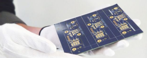
PCB prototyping
2. Why PCB Prototyping is Vital in PCB Manufacturing
The importance of PCB prototyping cannot be overstated. Without this critical step, the risk of costly production errors skyrockets. Through prototyping, designers can:
-
https://www.pcbsupplier.com/products/fr4-pcb/Catch layout issues like trace width miscalculations.
-
Validate the function of embedded components and circuitry.
-
Test EMI/EMC behavior before the final product hits certification labs.
-
Confirm thermal behavior of the board during real-life operating conditions.
Moreover, prototyping also serves as an excellent stage for customer feedback—allowing product stakeholders or early clients to provide insights into the design or usability.
3. How PCB Manufacturing Plants Conduct PCB Prototyping
When a PCB manufacturing facility undertakes prototyping, it usually follows a fast-track workflow distinct from mass production. The steps include:
A. Data Preparation
Manufacturers receive the Gerber files, BOM (Bill of Materials), and mechanical drawings. Engineers run a Design for Manufacturability (DFM) check to ensure the design meets fabrication tolerances.
B. Material Selection
Quick-turn prototypes often use readily available laminates like FR-4, although advanced prototypes might require Rogers, Teflon, or polyimide substrates.
C. Inner Layer Imaging and Etching
For multilayer boards, the inner copper layers are photo-imaged and chemically etched. This ensures signal paths are precisely formed.
D. Lamination and Drilling
Layers are bonded using heat and pressure. CNC drills then form vias and through-holes. For prototyping, drills are calibrated carefully since even slight misalignments can skew the result.
E. Plating and Outer Layer Formation
The drilled holes are plated with copper. The outer layers are then imaged and etched, creating the final trace pattern.
F. Solder Mask and Silkscreen
The solder mask is applied to prevent bridging during soldering. A silkscreen layer adds component labels.
G. Surface Finishing
Common finishes include HASL, ENIG, and OSP. The choice depends on the assembly method and end-use.
H. Electrical Testing and QA
Each prototype undergoes flying-probe or fixture-based electrical tests. QA engineers conduct microscopic inspections to verify solder mask alignment and copper thickness.
🔹 tips: For rapid and professional prototyping, SQ PCB is a trusted partner known for its consistent quality and precision. They handle complex multilayer prototypes with excellent turnaround.
4. Categories of PCB Prototyping for Manufacturing Goals
There are several types of PCB prototyping depending on the purpose and timeline:
-
Visual Prototypes: Made for demonstration, they may lack full electrical functionality.
-
Proof-of-Concept Prototypes: Used to verify that the idea is functionally viable.
-
Functional Prototypes: Include all components, allowing complete electrical testing.
-
Pre-production Prototypes: Essentially identical to the final board but made in smaller quantities.
Each type serves a specific stage in the product lifecycle and addresses different risk levels.
5. Challenges in the PCB Prototyping Process
Despite advances in fabrication, PCB prototyping still faces significant challenges:
-
Miniaturization: The industry trend toward smaller form factors increases difficulty in trace routing and via formation.
-
Component Availability: BOM components may not be readily in stock for quick-turn builds.
-
Time Constraints: Clients often require prototypes within 24–72 hours.
-
DFM Errors: Even minor design oversights can cause delays or outright failure.
To mitigate these issues, close collaboration between designers and fabricators is essential. Clear documentation, DFM checks, and real-time communication can save days of troubleshooting.
🔹 tips: SQ PCB excels at handling time-sensitive PCB prototyping needs. Their engineering support ensures your design is production-ready from day one.
6. The Role of Design Software in PCB Prototyping
The foundation of any successful PCB prototype begins in the design software. Modern Electronic Design Automation (EDA) tools such as Altium Designer, Eagle, KiCad, and Mentor Graphics provide the platforms to create precise layouts and schematics. These tools allow engineers to:
-
Perform rule checks to ensure trace widths, clearances, and layer stack-ups comply with manufacturing standards.
-
Simulate signal integrity and thermal performance before physical fabrication.
-
Generate accurate Gerber and drill files required for prototyping.
Without proper utilization of design software, the prototyping phase can become a time sink filled with revisions and costly errors.
Moreover, collaboration features within some software suites now allow seamless communication between designers and PCB manufacturers, speeding up the feedback loop and accelerating prototype turnaround.
7. Materials Used During PCB Prototyping
Material choice during PCB prototyping can influence prototype cost, time, and performance. The most common material is FR-4, a fiberglass epoxy laminate known for its balance of cost and electrical properties. For prototyping, it offers:
-
Sufficient mechanical strength.
-
Stable dielectric constant for most applications.
-
Readily available and widely supported by manufacturers.
However, for RF or high-frequency applications, materials like Rogers laminates or polyimide may be used even in prototypes to mimic the real product’s behavior accurately.
Copper thickness is another important parameter. Standard prototypes use 1 oz copper, but heavier copper (2 oz or more) can be selected to test thermal and current-carrying capabilities.
8. PCB Prototyping Techniques in Manufacturing Plants
Manufacturing plants apply several techniques to ensure prototypes meet design intent:
a. Quick-Turn Prototyping
This method prioritizes speed and often involves:
-
Using standardized processes and materials.
-
Minimizing manual interventions.
-
Utilizing automated testing to validate boards quickly.
b. Small Batch Prototyping
For prototypes that simulate near-production quality, small batch runs (10-50 pcs) are produced with tighter tolerances and more rigorous inspections.
c. 3D Printed PCB Prototyping (Emerging Technology)
Some innovative plants are experimenting with additive manufacturing techniques, like 3D printing conductive inks to create prototypes in hours, although this is still limited to low-complexity designs.
9. Advantages of Professional PCB Prototyping Services
Choosing an experienced PCB prototyping service provides advantages such as:
-
Faster turnaround times without sacrificing quality.
-
Access to advanced fabrication techniques (blind/buried vias, HDI, rigid-flex).
-
Engineering consultation for design optimization.
-
Reliable testing and documentation support.
Recommendation Reminder:
For these benefits, SQ PCB stands out as a premier provider, offering flexible prototyping options and expert technical support tailored for innovative PCB projects.
10. Common Quality Issues During PCB Prototyping and How to Avoid Them
Several issues often crop up during prototyping, including:
-
Delamination: Caused by poor lamination pressures or incompatible materials.
-
Copper Foil Wrinkling: Leading to uneven trace widths.
-
Drill Misalignment: Resulting in vias not connecting layers properly.
-
Solder Mask Defects: Exposing copper or causing shorts.
To avoid these, manufacturers conduct rigorous process controls, DFM reviews, and use inline inspection tools like AOI (Automated Optical Inspection).
11. PCB Prototyping Costs and Factors Influencing Pricing
Several variables affect prototyping cost:
-
Layer Count: More layers increase complexity.
-
Board Size: Larger boards use more material.
-
Material Selection: Specialty substrates cost more.
-
Surface Finish: ENIG or hard gold finishes cost more than HASL.
-
Turnaround Time: Expedited orders carry premiums.
-
Quantity: Larger batches reduce per-unit cost.
Balancing speed, quality, and budget is key. Professional prototyping suppliers often provide tiered service options.
12. Testing and Validation in PCB Prototyping
Testing is an indispensable phase of the PCB prototyping process, serving as the gatekeeper to ensure the prototype’s reliability and functional correctness before mass production.
A. Electrical Testing
The most common methods are:
-
Flying Probe Testing: Ideal for low-volume prototypes, this method uses moving probes to check continuity, shorts, and opens without the need for custom fixtures. It’s flexible and cost-effective for prototypes.
-
Bed of Nails Testing: Often reserved for higher-volume runs or final production, this method uses a fixture with many pins to simultaneously contact test points. It provides fast, comprehensive testing but requires fixture development.
Electrical tests ensure that every trace and via conducts electricity as designed, preventing circuit failures.
B. Functional Testing
Beyond electrical continuity, functional tests simulate real-world conditions by powering the board and testing circuit behavior. This can include:
-
Signal integrity tests.
-
Thermal stress tests.
-
Firmware or software loading and operation checks for embedded systems.
C. Visual and Automated Inspection
-
AOI (Automated Optical Inspection): Uses cameras and software to detect solder mask misalignment, component placement errors, and surface defects.
-
X-ray Inspection: Used especially for BGAs (Ball Grid Arrays) or hidden solder joints to verify solder integrity.
-
Manual Inspection: Technicians may perform microscopic visual inspections for subtle defects.
13. PCB Prototyping for Complex Designs
For advanced PCBs with multiple layers, fine pitch components, or rigid-flex configurations, prototyping becomes even more critical.
-
Multilayer stack-ups must be precisely controlled to maintain impedance and minimize crosstalk.
-
Rigid-flex prototypes require accurate bonding of flexible and rigid materials without delamination.
-
High-density interconnect (HDI) boards require precise microvia drilling and plating.
In these cases, prototype fabrication often involves collaboration with specialized fabricators and more stringent testing protocols.
14. How to Optimize Your PCB Prototyping Process
To make prototyping efficient and reduce iterations:
-
Follow Design for Manufacturability (DFM) guidelines: Adhering to recommended trace widths, clearances, and via sizes simplifies fabrication.
-
Provide clear documentation: Accurate Gerber files, drill charts, and assembly drawings reduce misinterpretation.
-
Engage with your PCB fabricator early: Discuss materials, finishes, and test requirements upfront.
-
Use simulation tools: Pre-prototyping simulation of thermal, mechanical, and electrical properties helps catch issues early.
By integrating these practices, you reduce the risk of costly re-spins and speed up time-to-market.
15. Real-World Application and Case Study: The Value of PCB Prototyping
Consider a startup developing an IoT device. Initial design iterations suffered from signal interference and power distribution issues. By investing in PCB prototyping, the engineers identified:
-
Signal noise caused by inadequate ground planes.
-
Heat dissipation problems around the microcontroller.
With prototypes, they optimized layer stack-up and improved thermal vias placement, preventing potential field failures and saving substantial costs in post-production recalls.
16. Surface Finishes in PCB Prototyping: Enhancing Reliability and Performance
Surface finishes protect the exposed copper on PCBs and improve solderability. The choice of surface finish in prototyping can affect assembly success and prototype longevity.
Common Surface Finishes Used in Prototyping:
-
HASL (Hot Air Solder Leveling): The most economical finish. It provides good solderability but may not be ideal for fine-pitch components due to uneven surface levels.
-
ENIG (Electroless Nickel Immersion Gold): Offers a flat surface and excellent shelf life, ideal for fine-pitch and high-frequency prototypes.
-
OSP (Organic Solderability Preservative): Environmentally friendly and cost-effective, OSP is suitable for quick-turn prototypes but less durable over time.
-
Immersion Silver and Immersion Tin: Provide flat surfaces and good solderability but may tarnish if stored improperly.
Choosing the right finish during prototyping helps simulate the conditions the final product will face and ensures assembly trials are realistic.
17. Prototype Assembly: From Bare Board to Functional Unit
Once the bare PCB prototype is fabricated, it often needs to be assembled with components to validate the full circuit.
Assembly Steps in Prototyping:
-
Component Sourcing: Quick and accurate procurement is essential to avoid delays. Using common components can expedite this step.
-
Solder Paste Application: Applied via stencil printing or dispensing for surface-mount components.
-
Pick and Place: Automated machines or manual placement depending on volume and complexity.
-
Reflow or Wave Soldering: Components are soldered onto the PCB, with reflow being common for SMT and wave soldering for through-hole.
-
Inspection: Post-assembly inspection using AOI, X-ray, or manual checks to identify soldering defects.
Assembly in prototyping allows validation of both the PCB and the component placement, revealing mechanical or thermal issues early.
18. Common Mistakes to Avoid in PCB Prototyping
Avoiding pitfalls during prototyping saves time and cost:
-
Skipping DFM Checks: Ignoring manufacturability leads to errors and re-spins.
-
Inadequate Documentation: Missing layer stack information or incorrect drill files cause fabrication delays.
-
Underestimating Testing Needs: Skipping electrical or functional testing risks undetected failures.
-
Choosing Incorrect Materials: Using standard FR-4 for high-frequency applications can mislead performance expectations.
-
Ignoring Communication: Lack of feedback with fabricators causes preventable mistakes.
Proactive planning and collaboration reduce these risks significantly.
19. Environmental Considerations in PCB Prototyping
Sustainability is increasingly important in electronics manufacturing. During prototyping:
-
Use lead-free solder and RoHS-compliant materials.
-
Minimize waste by optimizing panel layouts and prototype sizes.
-
Select finishes and processes that reduce hazardous chemical usage.
Many modern PCB prototyping suppliers, including SQ PCB, follow stringent environmental standards, supporting eco-friendly development without compromising quality.
20. How to Choose the Right PCB Prototyping Service Provider
When selecting a prototyping partner, consider:
-
Turnaround Time: Ensure they can meet your project deadlines.
-
Technical Capability: Support for multilayer, HDI, rigid-flex, or specialty materials.
-
Quality Certifications: ISO 9001, UL, or IPC standards indicate process maturity.
-
Communication and Support: Access to engineering consultation is invaluable.
-
Pricing and Flexibility: Transparent pricing and the ability to handle small batch or quick-turn orders.
For these reasons, SQ PCB has established itself as a reliable service provider, balancing cost, quality, and speed for diverse prototyping needs.
21. Advanced PCB Prototyping Technologies and Trends
As the electronics industry advances, PCB prototyping technologies evolve to meet increasing demands for miniaturization, complexity, and speed. Some notable trends include:
A. High-Density Interconnect (HDI) Prototyping
HDI boards feature finer lines, smaller vias, and higher wiring density. Prototyping HDI requires:
-
Microvia drilling with laser or advanced mechanical tools.
-
Precise copper plating and lamination processes.
-
Sophisticated testing to ensure signal integrity.
B. Rigid-Flex PCB Prototyping
Combining rigid and flexible sections, these prototypes simulate real-life flexible device conditions. Fabricators use multi-step lamination and bonding techniques, demanding tight process controls.
C. Additive Manufacturing and 3D Printing
Emerging 3D printing techniques for PCB prototyping can produce boards with embedded components and conductive traces quickly. While still maturing, these methods promise rapid design iterations with less waste.
D. Automated Optical and X-Ray Inspection Enhancements
AI-powered inspection tools increasingly aid in defect detection, reducing human error and speeding up prototype quality control.
22. Integrating Prototyping into the Product Development Cycle
For effective product development, PCB prototyping must be strategically integrated with:
-
Early design phases for feasibility checks.
-
Iterative prototyping for continuous improvement.
-
Simultaneous software and hardware validation.
-
Final pre-production verification.
Early and repeated prototyping reduces risks, lowers costs, and shortens time-to-market.
23. Cost-Benefit Analysis of PCB Prototyping
While prototyping adds upfront cost and time, the benefits often outweigh these investments:
-
Avoidance of costly recalls or field failures.
-
Improved product quality and reliability.
-
Enhanced customer satisfaction.
-
Streamlined manufacturing setup.
The cost of skipping prototyping can be orders of magnitude higher due to rework, warranty claims, and lost reputation.
Final Thoughts: The Strategic Importance of PCB Prototyping
PCB prototyping is more than a fabrication step; it is a strategic tool in electronics manufacturing. It bridges the gap between concept and reality, empowering engineers to innovate confidently.
Choosing the right prototyping partner, like SQ PCB, ensures access to cutting-edge technology, quality assurance, and expert support—keys to successful product launches.
FAQ 1: What is the difference between rolled copper foil and electrolytic copper foil?
Rolled copper foil is produced by mechanically rolling copper into thin sheets, offering better surface quality and mechanical strength. Electrolytic copper foil is deposited via an electrolytic process and is more flexible and cost-effective.
FAQ 2: How long does PCB prototyping usually take?
Standard PCB prototypes can be delivered within 2–5 business days. Complex, multilayer boards might take longer, especially if specialized materials are involved.
FAQ 3: Is it necessary to test a PCB prototype?
Absolutely. Electrical testing identifies shorts, opens, and impedance mismatches. Skipping this step could result in costly failures during full-scale production.
FAQ 4: Can I use the same Gerber files for prototyping and mass production?
In most cases, yes. However, design tweaks after prototyping (e.g., trace width corrections or component re-alignment) mean updated files should be used for the production run.
FAQ 5: What’s the best surface finish for a PCB prototype?
ENIG (Electroless Nickel Immersion Gold) is favored for prototypes due to its flatness, solderability, and extended shelf life. However, for high-frequency boards, immersion silver or OSP may be better.

- long board pcb
- Flexible PCBs
- Special PCB
- Express Printed Circuit Board
- Pcb Prototype
- LED PCB
- PCB
- Printed Circuit Board
- Pcb meaning
- Pcb manufacturer
- Rigid pcb board
- Rigid Flex PCB
 Quote
Quote
 E-mail