1. Introduction to Microwave PCB in High Frequency Circuits
In the realm of advanced electronics, especially those operating in the GHz frequency range, the term Microwave PCB has become increasingly prominent. But what does it truly encompass? A Microwave PCB refers to a printed circuit board specifically engineered for applications operating at microwave frequencies, typically above 1 GHz and extending up to 100 GHz and beyond.
Unlike conventional PCBs, Microwave PCBs are characterized by stringent requirements for material selection, fabrication tolerance, and electromagnetic performance. Their role is crucial in supporting reliable and efficient transmission of high-frequency signals, with minimal loss and distortion. These PCBs are the cornerstone of many modern systems including radar, satellite communications, aerospace electronics, 5G infrastructure, and automotive ADAS.
Why Microwave Frequencies Demand Special PCB Attention
As signal frequency increases, traditional assumptions about PCB behavior no longer hold. Conductors begin acting as antennas, substrates exhibit signal dispersion, and vias become unintended resonators. Therefore, Microwave PCB design must be approached with a deep understanding of electromagnetics, transmission line theory, and material science.
Microwave PCBs aren’t just about using different materials—they represent a paradigm shift in layout, fabrication, testing, and long-term performance. In my experience working with RF and microwave systems, even a seemingly minor imperfection—such as a misaligned microstrip—can render an entire system nonfunctional.
This introduction serves as a foundation for diving deep into the engineering and manufacturing world of Microwave PCB. Throughout the following sections, we will explore not only the technical framework but also the practical challenges and real-world solutions.
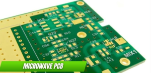
Microwave PCB
2. History and Evolution of Microwave PCB in High Frequency Circuits
The journey of Microwave PCB technology is intricately linked with the evolution of high-frequency electronics, beginning with early radar systems during World War II. At that time, vacuum tubes and bulky components dominated the landscape, and PCBs were rudimentary or non-existent. As systems moved toward miniaturization and higher frequencies, the need for specialized substrates and controlled impedance pathways became apparent, giving rise to what we now know as Microwave PCBs.
Early Developments: From Prototypes to Radar Modules
In the 1950s and 60s, as radar and aerospace technologies progressed, engineers began experimenting with polytetrafluoroethylene (PTFE)-based laminates to address signal loss issues. These materials—such as DuPont’s Teflon—offered stable dielectric properties at microwave frequencies. However, their softness and thermal expansion posed challenges for large-scale manufacturing.
The first true Microwave PCBs were hand-etched prototypes used in military applications, often mounted on rigid carriers to withstand mechanical stress. These boards were not mass-produced but provided critical functionality in systems where performance was more important than cost.
Microwave PCB Enters the Communication Era
The 1980s and 90s saw a boom in telecommunications, prompting the demand for cost-effective and scalable high-frequency solutions. During this time, Microwave PCB manufacturing matured with the introduction of new materials like Rogers RT/duroid® laminates, which featured low dielectric loss and higher thermal stability. Photolithographic processes also improved, enabling precise patterning of microstrip and stripline geometries.
During my early involvement in RF product development, I saw firsthand how transitioning from traditional epoxy-glass PCBs to microwave-grade laminates reduced insertion loss by over 50%—a game-changer for signal clarity in long-range transmitters.
Present Day: The Age of 5G, IoT, and Satellite Connectivity
In the 21st century, the development of 5G, autonomous vehicles, satellite constellations, and advanced radar systems has pushed Microwave PCB technology to new heights. Modern Microwave PCBs are now expected to support frequencies upward of 40 GHz, sometimes exceeding 70 GHz in mmWave designs.
Miniaturization, integration of active and passive components, and multilayer stackups are now the norm. The industry has also embraced hybrid designs—using a combination of materials such as FR-4 and ceramic-filled PTFE to balance cost and performance.
These changes have not only affected how Microwave PCBs are manufactured but also how they are simulated, tested, and qualified for reliability. Today’s development environments often integrate electromagnetic (EM) simulation tools and 3D layout validation to ensure performance before the first prototype is even built.
3. Fundamental Principles Behind Microwave PCB in High Frequency Circuits
Understanding the foundational science behind a Microwave PCB is essential to appreciating its role in high frequency circuit performance. Unlike standard PCBs that primarily focus on connectivity and component mounting, a Microwave PCB must act as a carefully engineered transmission medium for electromagnetic (EM) waves. Every physical feature—from trace width to substrate thickness—directly impacts the signal behavior at microwave frequencies.
Transmission Line Theory in Microwave PCB
One of the most critical principles at play in a Microwave PCB is transmission line theory. At frequencies above 1 GHz, PCB traces no longer behave like simple wires. Instead, they function as transmission lines that must maintain a constant impedance to prevent signal reflection and attenuation.
There are several types of transmission line structures commonly used in Microwave PCB designs:
-
Microstrip Lines: Conductive traces on the surface of the dielectric, with a ground plane beneath. Simple and easy to fabricate, but more prone to radiation losses.
-
Stripline Structures: Traces embedded between two ground planes, providing better shielding and impedance control.
-
Coplanar Waveguides (CPW): Traces surrounded by ground planes on the same layer, useful for minimizing radiation and crosstalk.
Designers must calculate the characteristic impedance (typically 50 ohms) using the dimensions of the conductor, the height of the substrate, and the dielectric constant (εr) of the material. Software tools are used extensively to simulate field distribution and optimize these parameters.
Dielectric Behavior at High Frequencies
Dielectric constant and dissipation factor are two key material properties that heavily influence Microwave PCB performance:
-
Dielectric Constant (εr) determines the speed at which EM waves propagate through the substrate. Variations in εr can cause phase distortion and impedance mismatches.
-
Dissipation Factor (Df) quantifies how much signal energy is lost as heat. Materials with low Df (e.g., Rogers RO4003C, Taconic RF-35) are ideal for high-frequency applications.
At microwave frequencies, even slight inconsistencies in εr can lead to signal skew, timing issues, or degraded signal-to-noise ratios. This is why specialized laminates with tightly controlled dielectric properties are indispensable in Microwave PCB design.
Skin Effect and Conductor Losses in Microwave PCB
Another phenomenon that becomes dominant at high frequencies is the skin effect—the tendency of alternating current to flow near the surface of a conductor. As a result, effective resistance increases with frequency, leading to additional signal loss.
To counteract this, designers use:
-
Smooth copper finishes (e.g., rolled annealed copper) to reduce surface resistance
-
Plated finishes like ENIG or silver for improved conductivity
-
Wider traces to compensate for higher resistance
Maintaining conductor integrity is critical to ensuring that a Microwave PCB performs well in demanding signal environments such as phased array antennas or mmWave transceivers.
4. Key Design Challenges of Microwave PCB in High Frequency Circuits
Designing a Microwave PCB presents a unique set of challenges that go far beyond those encountered in standard PCB layouts. The behavior of electromagnetic waves at microwave frequencies introduces complexities in layout geometry, material selection, and signal integrity that must be carefully managed from the outset. In this section, we explore the primary design difficulties engineers face when working with Microwave PCBs.
Maintaining Controlled Impedance
One of the most critical goals in Microwave PCB design is maintaining consistent impedance throughout the signal path. Unlike low-frequency designs where minor impedance mismatches might be tolerated, high-frequency signals are extremely sensitive to any variation in the physical trace geometry or dielectric consistency.
Challenges include:
-
Precise control of trace width and spacing
-
Tight manufacturing tolerances for dielectric thickness
-
Variability in substrate εr due to environmental factors (e.g., humidity, temperature)
Even a 5% deviation from the intended impedance can result in unacceptable reflection losses, standing wave formation, and degraded system performance.
Managing Signal Loss and Crosstalk
At microwave frequencies, signal attenuation occurs due to:
-
Conductor losses (exacerbated by skin effect)
-
Dielectric losses (dependent on Df)
-
Radiation losses (especially in microstrip lines)
Moreover, crosstalk between adjacent transmission lines becomes a major issue in dense layouts. Signals can couple inductively or capacitively, leading to signal corruption, phase delays, or even false triggering in digital systems.
Key mitigation strategies include:
-
Wider spacing between high-speed traces
-
Use of ground planes and via fences
-
Multilayer stackups to isolate signal layers
-
Incorporation of shielding where applicable
Thermal Management Constraints
While microwave signals themselves don’t always generate high heat, the active devices (e.g., power amplifiers, mixers, oscillators) on a Microwave PCB often do. Coupled with the thermal resistance of specialized materials, this can create significant heat dissipation challenges.
Thermal management approaches include:
-
Thermal vias and heat spreaders
-
Embedded copper coins
-
Metal-core or hybrid PCB structures
-
Use of thermally conductive but electrically insulating dielectrics
In high-power RF designs, neglecting thermal performance can lead to material delamination, impedance drift, or even catastrophic device failure.
Via Effects and Transition Losses
Vias, while essential for interlayer connectivity, behave unpredictably at microwave frequencies. A single via can introduce inductance, capacitance, and phase delay—creating a discontinuity that disturbs signal flow.
Key considerations include:
-
Minimizing via count on high-speed traces
-
Using blind or buried vias for smoother transitions
-
Implementing backdrilling to remove unused via stubs
-
Designing via arrays for effective ground returns
In my own design experience, using via stubs without backdrilling once led to a notch in the frequency response of a 5 GHz filter—a costly mistake in production.
Fabrication Tolerances and Repeatability
Unlike standard FR-4 boards, a Microwave PCB often uses materials such as PTFE, hydrocarbon ceramics, or low-loss composites. These materials are softer, more prone to movement during lamination, and require specialized handling. As a result, maintaining fabrication tolerances can be difficult.
Typical challenges include:
-
Material shrinkage or expansion
-
Uneven copper etching due to surface roughness
-
Difficulty in drilling and plating through soft substrates
-
Layer registration issues in multilayer designs
To ensure repeatability, manufacturers often use tight process controls, laser direct imaging (LDI), and automated optical inspection (AOI) to verify critical dimensions.
5. Dielectric Properties Considerations in Microwave PCB Design
Dielectric properties are a cornerstone of Microwave PCB performance. As operating frequencies rise into the GHz and mmWave range, the electrical behavior of the substrate’s dielectric material becomes increasingly critical. It not only governs how signals propagate but also determines how much energy is lost along the way. Without a solid understanding of these properties, even the best circuit designs can fall short of performance expectations.
Understanding Dielectric Constant (εr) in Microwave PCB
The dielectric constant (εr)—also known as relative permittivity—measures how much the substrate material slows down the signal relative to the speed of light in a vacuum. In a Microwave PCB, εr directly impacts:
-
The wavelength of the signal on the board
-
The impedance of transmission lines
-
Signal delay and timing skew
-
The ability to match high-speed interconnects
At microwave frequencies, signal behavior is not just affected by the nominal εr, but also by how stable and uniform it remains across:
For high-performance Microwave PCBs, substrate εr must remain as flat as possible over frequency. A shift in εr from 3.38 to 3.50 over a 10 GHz bandwidth may seem minor, but it can cause phase errors, impedance drift, and degradation in multi-channel systems.
6. Conductor Materials and Surface Finish in Microwave PCB
While dielectric materials form the structural and electrical base of a Microwave PCB, the choice of conductor materials and surface finishes plays an equally critical role in determining overall signal integrity and system performance at high frequencies. At microwave and millimeter-wave frequencies, current no longer flows uniformly throughout the entire cross-section of a conductor. Instead, due to the skin effect, current is confined to the outermost surface of the conductor, making conductor quality and finish incredibly significant.
The Skin Effect and Its Impact on Conductor Selection
At higher frequencies, the skin depth—the effective depth within which current flows—decreases. For instance, at 10 GHz, the skin depth in copper is roughly 0.66 μm. This means:
-
The majority of the current flows within this thin surface layer.
-
Surface roughness and plating quality dramatically affect conductor losses.
-
Losses increase as skin depth decreases with rising frequency.
The Microwave PCB must therefore use conductors with low resistivity and smooth surface finishes to minimize conductor loss.
Common Conductor Materials in Microwave PCB
1. Electrodeposited (ED) Copper
-
Most commonly used in standard PCB fabrication.
-
Offers a balance between performance and cost.
-
Typically rougher than other copper types, increasing conductor loss at high frequencies.
2. Rolled Annealed (RA) Copper
-
Produced by rolling and annealing, resulting in a smoother finish.
-
Lower surface roughness minimizes conductor loss.
-
Preferred in ultra-high-frequency Microwave PCB applications.
-
More expensive and mechanically delicate compared to ED copper.
3. High-Purity Copper Alloys
-
Used in very high-performance RF and microwave systems.
-
Examples: Copper-silver, copper-gold alloys.
-
Offers enhanced conductivity but higher material cost.
In practical terms, switching from ED copper to RA copper in a 40 GHz design can reduce conductor loss by as much as 20–30%, significantly improving power efficiency and signal quality.
7. Impedance Control in Microwave PCB Design
In high-frequency circuit design, impedance control is not optional—it is essential. In the realm of the Microwave PCB, where signals often operate in the GHz or even millimeter-wave ranges, any deviation from the designed impedance can result in severe signal degradation, reflection, and power loss. Achieving and maintaining precise impedance along every signal path is critical to ensuring signal integrity and overall system performance.
What is Impedance Control in a Microwave PCB?
Impedance, in simple terms, is the resistance a circuit offers to the flow of alternating current (AC), especially high-frequency signals. In a Microwave PCB, it specifically refers to the characteristic impedance of transmission lines—usually designed to be 50 ohms (or sometimes 75 ohms).
Controlled impedance ensures:
-
Maximum power transfer
-
Minimal signal reflection
-
Accurate phase and timing
-
Consistent signal quality across traces
Factors Affecting Impedance in Microwave PCB
Achieving accurate impedance is influenced by several physical and material-related parameters:
1. Trace Geometry
-
Width and thickness of the conductor line
-
Spacing between the signal trace and reference ground plane
-
For coplanar lines, gap between trace and adjacent ground
2. Dielectric Properties
-
Dielectric constant (εr) of the substrate
-
Consistency of εr across the board and frequency range
-
Dielectric thickness between signal trace and ground
3. Surface Finish and Copper Type
4. Manufacturing Tolerances
-
Laminate thickness variation
-
Etching accuracy of fine features
-
Plating control (especially in multilayer Microwave PCBs)
All of these must be tightly controlled to meet the targeted impedance, typically within a ±10% tolerance range, though tighter specs (±5%) are common for mission-critical RF applications.
Conclusion: Rethinking PCB Technology with Microwave PCB
The Microwave PCB is a cornerstone of high-frequency electronics, enabling advancements in telecommunications, defense, and IoT. By selecting the right materials, optimizing design, and leveraging precision manufacturing, engineers can push the boundaries of RF performance.
As 5G, satellite networks, and autonomous systems evolve, the demand for high-performance Microwave PCBs will only grow—making mastery of their fabrication essential for next-gen electronics. As we conclude this in-depth exploration of high-frequency circuit design, one theme stands out clearly: Microwave PCB technology has redefined the boundaries of traditional PCB design.
No longer can a printed circuit board be viewed merely as a passive mechanical platform that connects components. In the realm of microwave and millimeter-wave systems, the PCB itself becomes an active participant in signal propagation, electromagnetic behavior, and system-level performance.
our linkedin sqpcb.com

 Quote
Quote
 E-mail