1. Introduction to Etching in PCB Manufacturing
Etching is a foundational step in printed circuit board (PCB) fabrication, involving the selective removal of unwanted copper to define circuit patterns. Among the key approaches to this process are wet etching and dry etching—two distinctly different methods that serve similar end goals but via vastly different mechanisms and tools.
Both techniques are instrumental in shaping the final layout and functionality of PCBs, especially as the demand for miniaturization and high-performance electronics continues to grow.
Wet Etching vs. Dry Etching
2. Historical Background of Wet Etching vs. Dry Etching
The evolution of PCB etching techniques spans decades. Wet etching was the industry standard for much of the 20th century due to its simplicity and low cost. It typically involved chemical solutions like ferric chloride or ammonium persulfate to dissolve exposed copper.
Dry etching, on the other hand, emerged later as a response to the limitations of wet methods, particularly in terms of resolution and environmental impact. By utilizing plasma and reactive ion technologies, dry etching offered precision control and was better suited to high-density interconnect (HDI) and microvia applications.
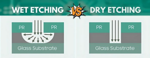
3. Basic Principles of Wet Etching vs. Dry Etching
At the core, wet etching is a chemical process, while dry etching is often physical or plasma-based. In wet etching, the copper layer is exposed to a liquid chemical reagent that dissolves the unwanted metal. It typically works isotropically, etching under the mask as well as downward, which can lead to pattern distortion in fine-line applications.
Dry etching, in contrast, uses gas-phase plasma to bombard the copper layer, selectively removing material through ionization and chemical reactions. It allows for anisotropic etching with finer resolution and cleaner edges—features increasingly vital in advanced PCB applications.
4. Chemical Mechanisms in Wet Etching vs. Dry Etching
In wet etching, common etchants include:
-
Ferric chloride (FeCl₃): An aggressive oxidizer that reacts with copper.
-
Cupric chloride (CuCl₂): Often used in regenerative systems.
-
Ammonium persulfate ((NH₄)₂S₂O₈): Offers cleaner etch profiles.
Dry etching utilizes gas-phase chemicals such as:
-
Chlorine-based gases (Cl₂, BCl₃): For copper removal.
-
Fluorine gases (CF₄, SF₆): In applications involving dielectric or silicon-based materials.
The reactions are carefully controlled under vacuum in a plasma reactor. This control minimizes undercutting and improves feature integrity.
5. Equipment and Process Setup in Wet Etching vs. Dry Etching
Wet etching systems are often simpler:
-
Spray or immersion tanks
-
Temperature-controlled baths
-
Chemical recirculation and filtration systems
Dry etching setups are more complex:
-
Plasma chambers with vacuum systems
-
RF power supplies
-
Gas mixing and flow controllers
-
Exhaust and scrubbing units
This difference in complexity has direct implications on both capital expenditure and maintenance requirements.
6. Materials Compatibility in Wet Etching vs. Dry Etching
Both methods have material-specific compatibilities. Wet etching can struggle with multilayer boards where precision is essential. Overetching can expose or damage inner layers, leading to performance degradation.
Dry etching, by virtue of its directionality and control, is more compatible with HDI boards, RF PCBs, and rigid-flex constructions. However, the aggressiveness of plasma can lead to issues with certain resins or substrate materials unless properly mitigated.
7. Cost Analysis of Wet Etching vs. Dry Etching
When it comes to upfront cost:
-
Wet etching wins due to its low-tech nature and less expensive setup.
-
Dry etching requires significant investment in equipment and infrastructure.
However, in terms of yield and precision:
-
Dry etching offers lower defect rates, especially for fine-line and high-density applications, which can translate into long-term savings.
8. Environmental Considerations of Wet Etching vs. Dry Etching
Wet etching generates chemical waste, which needs careful handling and disposal to avoid environmental damage. Managing ferric chloride or other corrosive agents poses challenges in compliance and safety.
Dry etching, although consuming gases and electricity, generally produces less liquid waste and is more environmentally sustainable when properly maintained.
9. Accuracy and Resolution in Wet Etching vs. Dry Etching
Dry etching offers superior line width control, critical for HDI and advanced PCB technologies. With anisotropic profiles, undercutting is minimized.
Wet etching’s isotropic behavior results in:
-
Less consistent line edges
-
Undercuts that affect impedance and signal integrity in RF boards
As a result, dry etching is preferred for designs <100 μm in feature size.
10. Throughput and Scalability in Wet Etching vs. Dry Etching
Wet etching scales well in volume manufacturing:
-
High-speed conveyor systems
-
Continuous processing capability
Dry etching is more limited in throughput due to:
-
Batch-based processing
-
Chamber cleaning and setup time
However, for specialized, low-volume, high-complexity boards, dry etching offers unmatched quality.
11. Applications in HDI and Advanced PCBs: Wet Etching vs. Dry Etching
For HDI PCBs with features like:
-
Microvias
-
Buried and blind vias
-
Fine trace routing
Dry etching is the dominant choice. The need for clean, high-resolution patterns in small areas makes wet etching obsolete for such applications.
That said, wet etching remains practical for simpler, larger-trace boards and consumer-level electronics where ultra-high resolution is not critical.
12. Reliability and Yield Comparisons: Wet Etching vs. Dry Etching
Dry etching systems can achieve higher yields due to their precision and lower process variability. However, they are more prone to equipment downtime and require stringent maintenance protocols.
Wet etching, though more forgiving in some respects, often suffers from:
-
Underetching or overetching
-
Mask lifting
-
Chemical contamination
These factors can reduce reliability in demanding applications.
13. Industry Trends Shaping Wet Etching vs. Dry Etching
With the rise of:
-
Wearables
-
IoT devices
-
5G infrastructure
-
Automotive electronics
There is a strong push toward dry etching to enable finer features and higher reliability. Nonetheless, the low cost of wet etching ensures it still holds a significant market share, especially in emerging economies and legacy product lines.
Conclusion: Evaluating Wet Etching vs. Dry Etching in the Era of PCB Innovation
The comparison between wet etching vs. dry etching in PCB manufacturing is not simply a matter of which is “better.” Instead, it is a question of application context, technical necessity, cost constraints, and future readiness.
Through the previous chapters, we explored the foundational chemistry, process mechanics, environmental implications, scalability, and real-world applications of both methods. Now, to conclude, we reflect on the core differentiators, summarize the strategic choices, and offer a forward-looking outlook for the PCB industry.
Key Differentiators: Wet Etching vs. Dry Etching
| Feature | Wet Etching | Dry Etching |
|---|---|---|
| Etching Profile | Isotropic (leads to undercut) | Anisotropic (vertical, precise) |
| Resolution | Limited to ~75–100 µm | Capable of <30 µm with low deviation |
| Throughput | Very high in continuous systems | Limited by batch processing |
| Material Compatibility | Good for FR-4, but limited for polyimide/flex | Excellent for advanced substrates |
| Environmental Impact | High liquid waste, water use | High energy, toxic gases, but less water |
| Cost | Lower initial investment | Higher CAPEX and OPEX |
| Use Cases | Mass-market, low-cost PCBs | HDI, RF, aerospace, medical, fine-line |
This table highlights how wet etching remains a strong solution for high-throughput, low-complexity products, while dry etching is the technology of choice for modern, advanced, and miniaturized PCBs.
When to Choose Which? A Practical Guide
Choose Wet Etching If:
-
Your product is in mass production with >75 µm traces
-
You need fast turnaround at minimal cost
-
You operate in an environment with sufficient chemical waste control
-
Your layers are limited to 2–8 and don’t include stacked microvias
Choose Dry Etching If:
-
Your design involves high-speed signals, RF structures, or controlled impedance
-
Your trace widths must go below 50 µm
-
Your board is multilayer HDI, rigid-flex, or polyimide-based
-
You must meet strict environmental or regulatory standards
The Role of Hybrid Strategies
More manufacturers are adopting hybrid workflows, using:
-
Wet etching for bulk material removal, especially outer layers
-
Dry etching for precision-critical layers, inner HDI layers, or microvia formation
This hybridization offers the best of both worlds—throughput and precision, economy and control—and will likely shape the future direction of many PCB fabrication shops.
Sustainability and Technological Convergence
The future of etching technology is deeply linked to sustainability, AI automation, and design complexity:
-
Cleaner chemistries and regenerative etching tanks will enhance wet etching’s eco-compatibility
-
Energy-efficient plasma systems and greener gases will reduce dry etching’s carbon footprint
-
AI-driven control systems will optimize both methods for higher yield and lower cost
-
Additive and subtractive hybrid manufacturing may redefine what “etching” even means
Thus, this isn’t merely a contest between two technologies—it is a dynamic evolution toward smarter, cleaner, and more adaptive PCB fabrication.
Etching, though a subtractive process by definition, plays a formative role in shaping the future of electronics. Whether through wet etching’s balance of scale and simplicity, or dry etching’s precision and sophistication, both remain pillars of the PCB industry.
The decision is not binary, but strategic. It depends on what kind of board you’re building, what your customers demand, and how you envision the future of your production line.
In the end, the smartest manufacturers will not choose sides—they will choose synergy.

- long board pcb
- Flexible PCBs
- Special PCB
- Express Printed Circuit Board
- Pcb Prototype
- LED PCB
- PCB
- Printed Circuit Board
- Pcb meaning
- Pcb manufacturer
- Rigid pcb board
- Rigid Flex PCB
 Quote
Quote
 E-mail