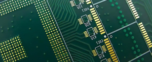
In the world of PCB design, few features are as critical as PCB pads. These small yet mighty conductive areas are where all the magic happens—they’re the very points where components connect, signals pass, and solder joints form. Whether you’re designing for surface-mount, through-hole, or high-density circuits, knowing the ins and outs of PCB pads is essential. In this guide, we’ll explore the various types of pads, design standards, layout rules, and common pitfalls. So, if you’re aiming for better solderability, stronger connections, and zero rework, read on—because PCB pad mastery starts here.
PCB Pads
1. Introduction to PCB Pads
What exactly are PCB pads, and why should you care? In short, a PCB pad is a defined area of exposed metal on a printed circuit board where a component’s lead, terminal, or pin is soldered.
But here’s the kicker… If your pad is too small, too misaligned, or poorly finished, the entire assembly process—and final product—could fail. Pads aren’t just little metal discs—they are mechanical anchors, electrical contacts, and thermal conduits all in one.
There are two broad categories of PCB pads: surface-mount (SMD) and through-hole (PTH). Both serve similar roles but are vastly different in construction, layout, and application. While traces carry the signal, the pad is where signal turns into function—where the component physically meets the board.
Let’s make it simple: no pads, no solder; no solder, no circuit.
| Pad Type | Description | Application |
|---|---|---|
| SMD Pad | Flat pad on PCB surface | Surface-mounted devices |
| Through-Hole Pad | Pad surrounding drilled hole | Leaded components |
| Thermal Relief | Pad with spokes | Connects to copper pour |
| Teardrop Pad | Tapered pad shape | Stress relief on corners |
2. Types of PCB Pads
Now let’s dive into the key types of PCB pads, each tailored for a specific purpose.
Surface-mount device (SMD) pads are flat rectangular or rounded copper areas used to anchor SMT components like resistors, capacitors, ICs, and more. These pads don’t go through the board, which allows for double-sided placement and compact designs.
Through-hole pads, on the other hand, are circular or oval pads with a central hole drilled through the board. These are used for components with leads—such as transformers, connectors, or diodes—often preferred in high-mechanical-strength applications.
But wait—there’s more! Thermal relief pads are essential in designs where large copper pours are connected to a pad. These pads include thin “spokes” that limit heat conduction during soldering, allowing easier solder reflow.
And don’t forget teardrop pads, which widen at the point where the trace meets the pad. Why? Because they reduce mechanical stress and improve drill alignment, especially during rework or flexing.
| Pad Type | Shape | Best Use |
|---|---|---|
| Rectangular | Flat, straight | SMD resistors, capacitors |
| Round | Circular | PTH components |
| Oval | Elongated round | Tight spacing |
| Teardrop | Tapered | Vibration or flex circuits |
Designing the right pad type can be the difference between success and failure—choose wisely!
3. PCB Pad Materials and Finishes
You might think a pad is just copper—but the finish matters just as much.
Let’s start with the base: most pads begin with copper. But raw copper oxidizes quickly, so manufacturers apply surface finishes to ensure good solderability and durability. This brings us to HASL, ENIG, OSP, and more.
But here’s the real story… Each finish affects how the pad behaves during soldering. HASL (Hot Air Solder Leveling) is common and economical but uneven. ENIG (Electroless Nickel Immersion Gold) offers a flat, reliable surface and longer shelf life—ideal for fine-pitch components and gold fingers.
OSP (Organic Solderability Preservative) is a lead-free, environmentally friendly option but more sensitive to oxidation.
| Finish | Type | Advantages | Drawbacks |
|---|---|---|---|
| HASL | Tin-lead or lead-free | Low cost, good solderability | Uneven surface |
| ENIG | Gold/Nickel | Flat, long-lasting, ideal for BGA | Higher cost |
| OSP | Organic layer | Eco-friendly, flat surface | Limited reworkability |
| Immersion Silver | Metal layer | High performance | Tarnishes easily |
Choosing the right finish ensures consistent solder joints and pad longevity in any environment.
4. SMD Pads: Design and Applications
SMD pads are the foundation of surface-mount technology, used across everything from smartphones to LED lights.
The pad shape depends on the component. For example, chip resistors use rectangular pads, while quad flat packages (QFPs) require precise spacing and sizing to match fine-pitch leads.
Ready for the good part? Poor SMD pad layout can cause tombstoning, where one side lifts during reflow, or bridging, where solder connects adjacent pads—causing shorts.
A successful SMD pad design follows IPC-7351 standards, ensuring optimal solder volume, pad length, and clearance.
| Component Type | Pad Shape | Recommended Pitch |
|---|---|---|
| 0603 Resistor | Rectangle | 0.8 mm |
| QFN Package | Center pad + perimeter | 0.5 mm |
| BGA | Grid array of pads | 0.4–0.8 mm |
Pad-to-pad spacing and correct alignment with solder masks are critical. Use a solder mask dam between pins to prevent solder bridging.
Design with reflow in mind—and your pads will stick the landing.
5. Through-Hole Pads: Function and Design Rules
Through-hole pads may seem old-fashioned in the age of surface mount, but they still play a critical role in high-current, high-mechanical-strength, and power supply designs.
So, what’s the real story? These pads must accommodate component leads, allow for solder to flow through, and still maintain structural and electrical integrity—on both sides of the board.
The relationship between hole size and pad size is vital. The pad must have an adequate annular ring—the copper surrounding the hole—to ensure proper connection and mechanical anchoring.
Let’s look at an example. A 0.8 mm component lead might require a 1.0 mm finished hole, with a 1.5 mm pad diameter, creating a 0.25 mm annular ring on all sides.
| Parameter | Recommended Value |
|---|---|
| Lead Diameter | 0.8 mm |
| Hole Size | 1.0 mm |
| Pad Diameter | 1.5 mm |
| Annular Ring | ≥0.25 mm |
Design rules also depend on copper weight, plating thickness, and whether the pad is connected to a plane (in which case thermal relief is essential).
Design it right, and through-hole pads will survive wave soldering, mechanical stress, and the test of time.
6. Pad Stackups in Multilayer PCBs
In multilayer PCBs, pad design becomes even more critical. Every pad is part of a pad stack—a vertical structure that includes top and bottom pads, internal layer connections, and via barrels.
But here’s the kicker… Not all pads in the stack are visible. Internal pads connect vias to power or ground planes. The wrong pad size here can cause signal integrity issues or even make your board unmanufacturable.
Modern designs may use via-in-pad, where vias are placed directly under component pads—common in BGAs and fine-pitch components. While this saves space, it also requires advanced processes like via plugging and planarization.
| Pad Stack Type | Use Case | Consideration |
|---|---|---|
| Through-hole stack | Standard PTH | Ensure sufficient annular ring |
| Blind via pad stack | HDI designs | Requires laser drilling |
| Via-in-pad | BGA, QFN | Increases cost but saves space |
Incorporate correct stack definitions in your CAD tool and coordinate with your fabricator early.
7. IPC Standards for Pad Design
When it comes to reliability, IPC standards are your safety net. IPC-7351 is the go-to guide for pad geometries, while IPC-2221 covers general PCB design standards.
But what’s the real story? These standards are based on years of industry data and help avoid the guesswork in pad sizing, especially when dealing with odd-shaped components or fine-pitch packages.
IPC standards define:
● Pad length and width based on lead geometry
● Courtyard areas for assembly clearance
● Solder mask and paste mask sizes
● Tolerances for reflow and wave soldering
| IPC Document | Purpose |
|---|---|
| IPC-7351 | SMT land pattern standard |
| IPC-2221 | Generic PCB design rules |
| IPC-A-600 | Acceptability of PCBs |
| IPC-610 | Acceptability of assemblies |
Following these standards ensures consistency, quality, and compatibility with automated assembly processes.
8. Pad Design for Solderability
Solderability starts with pad design. If a pad doesn’t wick solder properly or is blocked by solder mask, even the best components and solder paste won’t help.
Here’s where it gets interesting… Geometry plays a big role. Pads that are too small may not hold enough solder; those that are too large may cause wicking or dry joints.
You also need to consider solder mask clearance—leave at least 0.05 mm (2 mils) around each pad to prevent mask overlap. Add solder mask dams between adjacent pads (like on QFPs or BGAs) to prevent solder bridging.
| Factor | Ideal Value |
|---|---|
| Mask Clearance | ≥ 0.05 mm |
| Pad-to-pad Spacing | ≥ 0.2 mm |
| Dam Width (between pads) | ≥ 0.1 mm |
A well-designed pad means fewer defects, fewer reworks, and a rock-solid solder joint.
9. PCB Pads in High-Density Designs
In high-density layouts like mobile devices or HDI PCBs, space is at a premium. Pads must be designed smaller, closer, and cleaner than ever.
But here’s the kicker… As you reduce pad size, manufacturability drops and defect risks rise. That’s why many designers use micro pads (down to 0.3 mm) and fine-pitch spacing (less than 0.4 mm) with strict DFM (Design for Manufacturability) reviews.
To make it work, you may need via-in-pad, laser-drilled microvias, and tighter solder mask alignment. It’s not just layout—it’s a balance of electrical performance, mechanical integrity, and process capability.
| Metric | HDI Target |
|---|---|
| Pad Diameter | < 0.5 mm |
| Pitch (BGA, QFN) | 0.3–0.5 mm |
| Solder Mask Tolerance | ±0.025 mm |
Every mil matters—review with your manufacturer before production.
10. PCB Pad Defects and Failures
Let’s face it—pad problems are common. But they’re also preventable.
Common defects include lifted pads, which peel off due to excessive heat or poor lamination. Cold solder joints occur when solder doesn’t fully wet the pad, often due to contamination or oxidation. Bridging happens when solder connects adjacent pads unintentionally.
But the real story? Most failures come down to poor design or inadequate process control. Design wide enough pads, use correct finishes, and apply thermal relief where needed.
| Defect | Cause | Prevention |
|---|---|---|
| Lifted pad | Overheating, poor adhesion | Use good lamination + heat control |
| Cold joint | Oxidation or contamination | Use ENIG/OSP + proper storage |
| Solder bridge | Tight spacing | Increase pad spacing or use dams |
Quality starts at the pad—so don’t cut corners.
11. Thermal Pads and Heat Dissipation
Thermal pads aren’t your standard signal pads—they’re designed to move heat away from hot components and into the board’s thermal system.
What’s the real story? Without proper heat sinking, components like power ICs, FETs, or LEDs will overheat and fail. That’s where thermal pads come in. These are large, often central pads underneath the component package, typically connected to internal copper planes using thermal vias.
For example, a power regulator might require a 5×5 mm thermal pad with 9 thermal vias connecting to an internal copper pour. These vias act like vertical chimneys, conducting heat away efficiently.
| Feature | Recommendation |
|---|---|
| Pad Size | Same as exposed pad on component |
| Via Count | At least 9 (3×3 grid) |
| Via Diameter | 0.3–0.5 mm |
| Solder Mask | Tent top, open bottom |
Thermal pads reduce junction temperature, extend component lifespan, and are essential in automotive, industrial, and LED lighting applications.
12. Pad Sizing for Manual vs. Automated Assembly
Pad design isn’t one-size-fits-all—assembly method matters.
Manual soldering is more forgiving and benefits from larger pads, allowing technicians to apply heat and solder more easily. For example, a 1206 component soldered by hand might use pads 1.8 mm long, whereas automated reflow may need only 1.4 mm.
But here’s the kicker… If your board will go through automated pick-and-place and reflow, pad sizes must match IPC-7351 land pattern standards. That includes stencil openings, solder paste volume, and alignment tolerances.
| Assembly Type | Pad Sizing Style | Pad Example (1206) |
|---|---|---|
| Manual Soldering | Larger pads, more spacing | 1.8 mm x 1.5 mm |
| Reflow Soldering | Standard IPC pattern | 1.4 mm x 1.0 mm |
| Wave Soldering | Elongated pads | 2.0 mm x 1.5 mm |
Get this right, and you’ll minimize tombstoning, solder bridging, and placement errors.
13. Teardrop Pads and Their Benefits
This is where form meets function. Teardrop pads widen the trace-to-pad junction, reducing stress and improving manufacturability.
Ready for the good part? When a trace meets a round pad at a sharp angle, stress concentrates at that junction. In dynamic environments—flex boards, automotive, aerospace—this can lead to cracks or open circuits. Teardrop pads solve this by tapering the transition, distributing mechanical and thermal stress.
They also help with drill misalignment. If the drill hole is slightly off-center, a teardrop shape ensures the copper remains connected.
| Benefit | Description |
|---|---|
| Stress Relief | Less strain on pad-trace junction |
| Drill Tolerance | Prevents breakout due to offset |
| Aesthetic | Cleaner, more professional layout |
| Flex Support | Reduces cracking in flex circuits |
Use them on vias, through-hole pads, and sensitive signals—especially in mission-critical boards.
14. Software Tools for PCB Pad Design
Let’s talk tools—because manual design isn’t scalable.
Modern PCB CAD software offers robust libraries and automation for pad design. Tools like Altium Designer, KiCad, Eagle, and OrCAD let you define pad stacks, associate them with component footprints, and preview 3D assembly.
But here’s where it gets interesting… Advanced software also includes DFM checks, solder mask validation, and thermal simulation, helping you catch pad issues before they reach production.
| Tool | Strength | Pad Features |
|---|---|---|
| Altium Designer | Enterprise-class | Pad stacks, IPC wizard, 3D |
| KiCad | Free/open source | Custom pad shapes, scripting |
| Eagle | Lightweight | Simple SMD pad tools |
| OrCAD | Industrial grade | DRC, net connectivity analysis |
Use templates and IPC libraries to standardize pads across your designs and avoid reinventing the wheel.
15. Choosing a Manufacturer for Pad-Intensive Boards
Not all PCB fabricators are created equal—especially when your design includes tiny pads, fine-pitch components, and thermal relief features.
The real story? A good manufacturer will help you optimize pad design for their process. A great one will catch problems before they cost you money.
Look for manufacturers with:
● Capability to produce <0.2 mm pads
● ENIG, OSP, and immersion silver finishing
● 100% AOI and electrical testing
● DFM feedback during prototype reviews
Ask for their pad-to-hole tolerances, solder mask registration capability, and max copper weight per pad.
| Question | Why Ask It |
|---|---|
| What’s your min pad size? | Ensures pad resolution support |
| Do you inspect all pads? | Quality assurance |
| Can you handle via-in-pad? | Needed for dense BGA designs |
| Do you provide DFM reports? | Prevents pad-related errors |
Partner with a manufacturer who understands the nuance of pad design—and your products will thank you.
Conclusion
From SMD to through-hole, thermal to teardrop, PCB pads are far more than copper circles—they’re the lifelines of your circuit. Designing them properly means stronger solder joints, better thermal performance, and fewer production headaches. This guide covered the full pad design spectrum: materials, IPC standards, high-density layouts, common defects, and the tools and vendors you need to get it right. Whether you’re hand-soldering a prototype or sending a million boards to contract manufacturing, pad quality can make or break your entire build. Respect the pad, master the details, and your PCBs will reward you with reliability and performance.
FAQ Section
Q1: What is a PCB pad?
A PCB pad is a conductive area on a PCB that allows a component lead or terminal to be soldered to the board.
Q2: How does pad shape affect soldering?
Pad shape influences solder flow and joint strength. Rounded and teardrop pads often improve reliability.
Q3: What are the different types of PCB pads?
Common types include SMD pads, through-hole pads, thermal pads, and teardrop pads.
Q4: Why do some pads lift off the PCB during rework?
Excessive heat, poor adhesion, or weak lamination can cause pads to detach from the PCB substrate.
Q5: What is a thermal relief pad?
A thermal relief pad helps control heat during soldering by connecting to copper pours with narrow traces.

- long board pcb
- Flexible PCBs
- Special PCB
- Express Printed Circuit Board
- Pcb Prototype
- LED PCB
- PCB
- Printed Circuit Board
- Pcb meaning
- Pcb manufacturer
- Rigid pcb board
- Rigid Flex PCB
 Quote
Quote
 E-mail