1. Introduction to Surface Finishes in PCB Manufacturing
Surface finishes in PCB manufacturing play a critical role in ensuring solderability, oxidation resistance, and electrical connectivity. These finishes not only protect exposed copper traces but also influence long-term performance and cost. Among the numerous options available, Hard Gold vs ENIG (Electroless Nickel Immersion Gold) are two widely adopted solutions for specific applications, often misunderstood due to their similar appearances. This article aims to thoroughly dissect the differences between Hard Gold vs ENIG in both technical and practical dimensions.
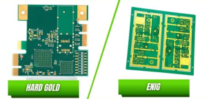
Hard Gold vs ENIG
Printed Circuit Board (PCB) manufacturing involves various surface finish options, each with distinct advantages and limitations. Among these, Hard Gold vs ENIG (Electroless Nickel Immersion Gold) are two prominent choices that significantly impact PCB performance, durability, and cost. This article explores the key differences between these finishes, their applications, and the factors influencing their selection in modern electronics.
1. Understanding Hard Gold in PCB Manufacturing
1.1 Composition and Deposition Process
Hard gold, also known as hard electrolytic gold, is deposited through an electroplating process. It consists of a layer of gold alloyed with small amounts of cobalt or nickel, enhancing its hardness and wear resistance.
1.2 Key Advantages of Hard Gold
-
Exceptional durability – Ideal for high-wear applications such as connectors and switches.
-
Superior conductivity – Ensures reliable signal transmission in high-frequency circuits.
-
Long shelf life – Resistant to oxidation and environmental degradation.
1.3 Limitations of Hard Gold
-
Higher cost – Due to the significant gold content and electroplating process.
-
Thicker deposition required – May lead to uneven surfaces if not properly controlled.
2. Overview of Hard Gold vs ENIG in PCB Applications
When choosing between surface finishes, designers must weigh trade-offs between durability, solderability, and cost. Hard Gold, also known as electroplated gold, is preferred for edge connectors and mechanical contact surfaces due to its robustness. ENIG, by contrast, is renowned for its flatness and excellent solderability, making it ideal for fine-pitch components and BGA pads. Both finishes serve different ends of the application spectrum.
In my experience working with both finishes in high-speed digital designs and ruggedized industrial systems, the functional split between Hard Gold vs ENIG becomes evident during the design-for-manufacturability phase.
3. Chemical Composition Differences in Hard Gold vs ENIG
At the molecular level, the distinction between Hard Gold vs ENIG begins with their chemical formulations:
-
Hard Gold typically includes a layer of nickel followed by electroplated gold that contains cobalt or other hardening agents. This results in a relatively thick and wear-resistant surface.
-
ENIG involves an electroless deposition of a nickel layer, followed by a thin immersion gold layer (usually less than 5µin). The gold here is soft and serves mainly as an anti-oxidation barrier for the nickel layer beneath.
This composition difference leads to significant variations in mechanical behavior, which I find especially relevant when selecting a finish for exposed edge contacts or wire-bonded regions.
4. Performance Characteristics of Hard Gold vs ENIG
The performance metrics of Hard Gold vs ENIG diverge most notably in the areas of wear resistance and contact durability:
-
Hard Gold: Excellent for repetitive mechanical contact; it can endure thousands of mating cycles without significant degradation. However, its thick gold plating can introduce cost and brittleness if misapplied.
-
ENIG: Offers superior planarity and solder wetting, but lacks the same endurance under mechanical abrasion.
Engineers must consider these differences not only in testing conditions but also in anticipated real-world usage. I’ve seen failures in prototypes where ENIG was used for card-edge connectors—a classic mismatch in application.
5. Manufacturing Processes of Hard Gold vs ENIG
The production processes of Hard Gold vs ENIG are fundamentally different:
-
Hard Gold is applied via electroplating, which requires precision masking and selective plating tanks. This increases process complexity but allows the deposition of thick layers (10µin to over 50µin).
-
ENIG is a chemical process that deposits a uniform nickel layer through electroless plating, followed by an immersion gold layer. It is more compatible with automated PCB lines and results in excellent pad flatness.
These differences influence manufacturing lead time and yield. In a mass production context, ENIG provides better consistency across panels, whereas Hard Gold requires tighter process control and dedicated masking steps.
6. Cost Considerations for Hard Gold vs ENIG
When evaluating Hard Gold vs ENIG for PCB manufacturing, cost is one of the most immediate and influential factors in the selection process. Although both surface finishes involve the use of gold—a relatively expensive raw material—the manner in which gold is deposited, and the required thickness, dramatically influence overall pricing.
Material Usage and Thickness Impact
The most direct contributor to cost difference lies in the gold thickness applied:
-
Hard Gold typically uses 10–50 microinches (µin) or more of electroplated gold, especially for edge connectors and wear-prone contacts. Because electroplating allows for thicker coatings, the volume of gold consumed is substantially higher.
-
ENIG, by contrast, applies a thin gold layer of 1–5 µin, mainly to protect the underlying nickel from oxidation prior to soldering.
As a result, the gold consumption per square inch of board area is significantly lower in ENIG, which translates into reduced material costs.
In projects I’ve led where cost containment was critical, shifting from Hard Gold to ENIG in non-contact applications offered immediate savings—often as much as 20–40% depending on board complexity and gold area coverage.
Process Complexity and Line Requirements
From a manufacturing operations standpoint, Hard Gold requires additional steps and specialized plating lines. Electroplating needs:
-
Selective gold application (often using tape masking or photoresist)
-
Longer process times for thicker deposits
-
Precision current control and maintenance of gold concentration in baths
This level of complexity not only increases labor and equipment costs but also introduces greater risk of process variability.
On the other hand, ENIG is more compatible with fully automated production lines, particularly those designed for high-volume PCB manufacturing. Its chemical process lends itself to batch treatment, offering higher throughput and lower labor overhead.
In my experience, this makes ENIG the go-to choice for mid-to-large volume production runs where consistent quality, cost-efficiency, and speed are critical.
Maintenance and Waste Management
Another often-overlooked cost factor in Hard Gold vs ENIG comparison is waste disposal and bath management:
-
Hard Gold baths require frequent maintenance, and gold recovery systems must be installed to capture waste particles and plating residues. This adds long-term environmental management costs.
-
ENIG also involves gold, but in much smaller quantities and with less frequent bath maintenance. Waste treatment costs are typically lower.
For smaller fabrication facilities or contract manufacturers with limited environmental handling capabilities, ENIG offers logistical and compliance advantages.
Application-Specific ROI
It is important to note that Hard Gold’s higher upfront cost can be justified in specific scenarios—particularly where durability and wear resistance translate into longer product life cycles or reduced service costs.
For instance, in military or aerospace equipment that may undergo frequent plug/unplug cycles, the premium paid for Hard Gold may result in lower total cost of ownership over a 10–20 year product lifespan.
Conversely, for consumer electronics or disposable medical devices, ENIG is nearly always more cost-effective due to lower functional demands and shorter usage cycles.
7. Wear Resistance Comparison in Hard Gold vs ENIG
One of the most significant functional differences between Hard Gold vs ENIG lies in their respective wear resistance capabilities. This distinction becomes especially critical in applications involving frequent mechanical contact, such as edge connectors, keypads, or sliding interfaces.
Mechanical Durability of Hard Gold
Hard Gold—electroplated gold alloyed with elements like cobalt or nickel—is specifically engineered to withstand repetitive physical abrasion. The hardness of this surface finish ranges from 130 to 200 Knoop, depending on the plating parameters and alloy composition. This high hardness allows it to:
-
Survive thousands of insertion/removal cycles in card-edge connectors
-
Resist surface deformation caused by mating contacts
-
Maintain electrical integrity over long periods, even in harsh environments
In real-world product testing, I’ve witnessed Hard Gold contact pads function flawlessly after 10,000+ insertion cycles without significant degradation, making it a favorite in enterprise-grade servers, military radios, and industrial control systems.
ENIG and Its Limitations Under Mechanical Stress
In contrast, ENIG (Electroless Nickel Immersion Gold) is not designed for abrasion resistance. The immersion gold layer is very thin (typically 1–3 µin) and primarily serves as a temporary protective coating for the underlying nickel layer, which itself is more susceptible to wear compared to hardened gold.
Under mechanical stress or frequent contact, ENIG surfaces exhibit:
-
Gold layer erosion after a relatively low number of contact cycles (as few as 50–100 insertions in some cases)
-
Nickel oxidation upon exposure if the gold layer wears off, which may increase contact resistance
-
Microscopic cracking or flaking under sliding or vibrating interfaces
For these reasons, ENIG is generally unsuitable for any high-cycle interface applications. I’ve encountered field failures in handheld devices where ENIG was mistakenly specified for buttons or connectors—resulting in rapid contact degradation and signal loss.
Visual and Structural Indicators of Wear
Under microscopic analysis, the differences in wear performance between Hard Gold vs ENIG become visually evident:
-
Hard Gold surfaces show minimal pitting or scoring even after extended use.
-
ENIG surfaces quickly display wear tracks, discoloration, or exposure of base nickel.
In quality assurance settings, surface profilometry and contact resistance testing often confirm what engineers already suspect from empirical results: ENIG lacks long-term durability under frictional load.
Relevance in Product Lifecycle Planning
For projects where the product is expected to endure multiple connection cycles over a long deployment period, Hard Gold is often the only viable choice. This includes applications such as:
-
Backplane connectors
-
Test probe contacts
-
Ruggedized communication systems
Meanwhile, in devices where connections are rare or permanent, ENIG provides sufficient performance at a lower cost.
In my own design decision matrices, I routinely map wear life requirements against finish options, and this analysis nearly always justifies the additional expense of Hard Gold for contact-intensive components.
8. Solderability Differences in Hard Gold vs ENIG
While wear resistance favors Hard Gold in mechanical applications, solderability is another vital dimension in the Hard Gold vs ENIG comparison. Solderability directly affects assembly quality, reflow reliability, and the long-term electrical performance of PCBs.
Solderability Characteristics of ENIG
ENIG (Electroless Nickel Immersion Gold) is widely praised in the electronics industry for its exceptional solderability. Its structure—a thin gold layer over a nickel base—offers several benefits in assembly processes:
-
Excellent wetting during reflow soldering, even with fine-pitch components
-
Flat surface finish, ideal for BGA pads, QFNs, and fine-line SMT components
-
Oxidation resistance prior to soldering, ensuring long shelf life
One of the most practical advantages of ENIG is its compatibility with lead-free soldering processes. Because of its planar surface and lack of microvoids, ENIG finishes typically outperform HASL or OSP in terms of joint integrity and consistency in reflow ovens.
In my experience assembling dense multi-layer boards with 0.4 mm pitch BGAs, ENIG outperforms nearly every other finish in terms of solder joint reliability. It remains the default choice in high-density consumer electronics and high-speed networking boards.
Solderability Limitations of Hard Gold
Despite its mechanical strengths, Hard Gold is not typically recommended for soldering, especially when compared to ENIG. The reasons include:
-
Thicker gold layers (especially above 20 µin) tend to dissolve into the solder and create brittle intermetallic compounds, such as AuSn₄
-
These brittle phases can cause microcracks, cold joints, or even joint fracture over thermal cycling
-
Surface roughness from electroplating may also interfere with solder wetting
In high-reliability applications, soldering onto Hard Gold pads is considered a design risk, and many assembly engineers prefer to avoid soldering directly on Hard Gold unless the gold thickness is tightly controlled (<5 µin, which begins to resemble ENIG specifications anyway).
In some edge cases, I’ve used selective plating, where Hard Gold is applied only to contact fingers, while solderable surfaces like component pads are finished with ENIG or HASL to maintain solderability.
Rework and Reliability Implications
Another key distinction in the Hard Gold vs ENIG discussion is how the two finishes behave during rework:
-
ENIG can generally tolerate limited rework if thermal cycles are controlled. The gold layer dissolves readily into the solder without forming large brittle phases due to its low thickness.
-
Hard Gold, if reflowed or soldered multiple times, may create cumulative intermetallic layers that degrade solder joint performance.
For projects that may require field repairs, rework, or hot air solder leveling post-assembly, ENIG is the more forgiving and reliable choice.
Practical Soldering Scenarios
Here are a few example scenarios I’ve encountered that highlight the real-world differences:
-
Scenario 1: A wearable health device used ENIG for its BGA connections, resulting in consistent solder ball formation and minimal voiding.
-
Scenario 2: A prototype used Hard Gold pads for all functions, including soldered ICs. The result was widespread brittle joints, leading to hairline fractures during testing.
9. Hard Gold vs ENIG in Edge Connector Design
One of the most critical application domains in the Hard Gold vs ENIG comparison is the design of edge connectors—the interface points where PCBs repeatedly mate with sockets, daughterboards, or card-edge contacts. In this context, surface finish choice is not just a question of cost or process convenience—it is a defining factor for product reliability and durability.
Functional Demands of Edge Connectors
Edge connectors are expected to:
-
Withstand repeated mating cycles (often thousands over the product’s life)
-
Maintain low contact resistance
-
Resist wear, oxidation, and surface contamination
-
Function reliably under varying mechanical pressures and environmental conditions
Because these requirements involve mechanical abrasion and long-term electrical stability, the surface finish must be carefully selected.
Why Hard Gold is the Default for Edge Connectors
Hard Gold is the industry standard for edge connectors for several compelling reasons:
-
Superior Wear Resistance
Hard Gold is electroplated with a gold-cobalt or gold-nickel alloy, which greatly increases its hardness (130–200 Knoop). This ensures:-
High cycle endurance (often >10,000 insertions)
-
Consistent surface integrity under pressure and friction
-
Stable electrical connectivity with low resistance
-
-
Customizable Thickness
The plating thickness can be adjusted based on durability requirements, typically ranging from 30–50 µin of gold over 100–200 µin of nickel. Designers can specify heavier plating for high-reliability applications. -
Corrosion Resistance
The noble metal composition offers excellent protection against oxidation and environmental degradation—crucial in industrial, automotive, and aerospace systems. -
Clean Contact Points
Hard Gold surfaces remain smooth, clean, and conductive, even after multiple insertions, which is critical in data transfer or power delivery through the connector interface.
In numerous high-reliability projects I’ve worked on—ranging from telecom routers to avionics control boards—Hard Gold plating was non-negotiable for edge contact zones. The costs were accepted because the risk of intermittent contact failure would be catastrophic.
Why ENIG Is Unsuitable for Edge Connectors
Although ENIG offers excellent solderability and is widely used for SMT pads, it is inappropriate for edge connectors due to the following limitations:
-
Low Wear Resistance
ENIG’s gold layer is typically 1–3 µin thick, deposited through immersion, not electroplating. It is too soft to endure even 50–100 mating cycles without:-
Rapid wear-through to the nickel layer
-
Increased contact resistance
-
Surface degradation and discoloration
-
-
Nickel Exposure and Oxidation
Once the thin gold layer wears away, the exposed nickel:-
Oxidizes quickly, increasing resistance
-
Loses its smoothness, leading to poor contact reliability
-
-
Lack of Mechanical Durability
The ENIG finish is designed for static soldered connections, not repeated mechanical engagement. Using ENIG for an edge connector is a design flaw, often leading to premature field failure.
In one real-world case, a consumer electronics product I reviewed used ENIG for a plug-in battery connection pad. After only 500 insertion cycles, we observed severe nickel exposure, dark tarnish, and intermittent power delivery—resulting in product returns and costly rework.
Design Best Practices: Mixed-Finish Strategy
In modern PCB design, it’s common—and recommended—to combine both finishes for optimal performance:
-
ENIG is used for component solder pads and signal lines.
-
Hard Gold is applied selectively to edge connector fingers, using masking and dedicated plating steps.
This approach maintains manufacturability and cost-efficiency, while ensuring durability where needed most.
Connector Geometry and Finish Coverage
When applying Hard Gold, designers must pay attention to:
-
Chamfered edges at the connector region for easy insertion
-
Defined plating boundaries, ensuring gold covers only the required zones
-
Solder mask clearance, avoiding unwanted interaction with the plating tanks
In my designs, I typically specify 45° edge chamfering and minimum 30 µin Hard Gold plating over nickel, with IPC Class 2 or Class 3 standards depending on the application criticality.
10. Future Trends and Innovations in Hard Gold vs ENIG Technologies
As PCB manufacturing evolves, both Hard Gold and ENIG technologies face ongoing innovation driven by demands for higher performance, environmental sustainability, and cost efficiency. This section explores emerging trends, new materials, and process advancements shaping the future landscape of these surface finishes.
Advanced Plating Processes
-
Pulse Plating and Nanotechnology for Hard Gold
-
Pulse plating techniques modulate current during electroplating to produce denser, more uniform Hard Gold layers with improved hardness and reduced internal stress.
-
Nanostructured gold alloys enhance wear resistance and electrical conductivity.
-
Early adopters report extended connector lifetimes and smoother finishes, enabling finer pitch edge contacts.
-
Enhanced Electroless Nickel Formulations in ENIG
-
New electroless nickel baths with reduced phosphorus content improve nickel grain structure, mitigating the risk of black pad and increasing corrosion resistance.
-
Additives in immersion gold solutions enable thicker, more uniform gold layers without increasing costs dramatically.
These process improvements aim to address traditional weaknesses in ENIG, allowing broader use in high-frequency and harsh environment applications.
Environmental and Regulatory Innovations
-
Cyanide-free Hard Gold plating chemistries are under development to reduce hazardous waste and simplify environmental compliance.
-
Closed-loop recycling systems for gold recovery in plating lines improve sustainability and reduce raw material costs.
-
ENIG processes continue evolving with lower-temperature baths and reduced chemical usage to minimize energy consumption and wastewater toxicity.
Manufacturers adopting these greener technologies are better positioned for compliance with increasingly stringent international regulations.
Alternative Surface Finishes Blurring Lines
-
Electroless Nickel Electroless Palladium Immersion Gold (ENEPIG) is gaining traction as a hybrid finish combining the hardness and solderability benefits of multiple layers.
-
Soft gold plating combined with advanced protective coatings offers wear resistance without Hard Gold’s brittleness.
-
Emerging graphene and other 2D-material coatings promise ultra-thin, highly conductive, and corrosion-resistant finishes that could revolutionize surface treatments.
Digital Manufacturing and Quality Control
-
AI-driven real-time plating bath monitoring enables tighter control over deposition parameters, reducing defects such as black pad or uneven gold thickness.
-
Advanced non-destructive testing (NDT) methods, including hyperspectral imaging and machine learning analysis, improve surface finish inspection accuracy.
These technologies improve yield, reduce waste, and support rapid production scaling.
My Perspective on Future Direction
I anticipate that Hard Gold and ENIG will coexist, but the boundary between their applications will narrow as innovations deliver higher performance, environmental compliance, and cost savings. Hybrid finishes and smarter plating controls will allow designers to customize surface finishes precisely to application needs, reducing overengineering and resource waste.
Staying informed about these trends is critical for engineers and procurement teams aiming to future-proof their PCB designs.
Conclusion
The comparison between Hard Gold vs ENIG surface finishes in PCB manufacturing highlights the nuanced trade-offs between mechanical durability, solderability, cost, environmental impact, and application suitability. Each finish offers unique advantages that cater to specific requirements:
-
Hard Gold excels in providing robust wear resistance and long-term mechanical reliability, making it indispensable for edge connectors and high-cycle mating surfaces. Its thicker gold layer and harder alloy composition deliver exceptional protection against abrasion and corrosion but come with higher costs and more complex environmental considerations.
-
ENIG, by contrast, offers excellent solderability, smooth surface finish, and cost efficiency, favored for general-purpose PCB pads in consumer and industrial electronics. While thinner and less wear-resistant than Hard Gold, ongoing innovations are improving its durability and reducing failure risks such as black pad syndrome. ENIG’s environmental footprint is generally lighter, aligning with growing sustainability demands.
A well-informed PCB designer or engineer must consider:
-
The mechanical stresses the PCB will endure, especially at connector interfaces.
-
The soldering and rework requirements of the assembly process.
-
The budgetary and environmental constraints imposed by the project.
-
The availability of reliable fabrication resources for each finish.
Integrating these factors leads to an optimized surface finish strategy, often blending both finishes to capitalize on their strengths while mitigating weaknesses.
Ultimately, the decision between Hard Gold and ENIG is a balancing act—one that influences product quality, lifecycle performance, manufacturing efficiency, and cost-effectiveness. Staying abreast of evolving technologies and maintaining close collaboration across design and manufacturing teams ensures the chosen finish aligns perfectly with the product’s functional and commercial goals.

- long board pcb
- Flexible PCBs
- Special PCB
- Express Printed Circuit Board
- Pcb Prototype
- LED PCB
- PCB
- Printed Circuit Board
- Pcb meaning
- Pcb manufacturer
- Rigid pcb board
- Rigid Flex PCB
 Quote
Quote
 E-mail