A 6 layer PCB stackup is one of the most widely used configurations in modern electronics, offering superior performance, high-density routing, and robust design flexibility. But here’s the kicker: understanding the design, benefits, and best practices of 6 layer PCBs can make a world of difference in how well your products perform. Whether you’re developing high-speed circuits or preparing for a large-scale manufacturing run, a solid grasp of the 6 layer PCB stackup process is essential.
In this article, we will explore everything you need to know about 6 layer PCB stackups, from their structure and components to the best practices and real-world applications. By the end, you’ll be equipped with the knowledge to optimize your designs and manufacturing processes, ensuring high-performance, reliable PCBs that meet your technical and economic goals.
6 Layer PCB Stackups
1. Introduction to 6 Layer PCB Stackup
A 6 layer PCB stackup refers to a printed circuit board design that consists of six layers of conductive and insulating materials stacked together to create a multi-layered board. These boards are typically used in more complex and high-performance applications where increased density and reduced space are crucial. What’s the real story? The additional layers in a 6 layer PCB enable the design of high-speed, compact circuits that are not possible with simpler stackups like 2-layer or 4-layer designs.
The six layers in a 6 layer PCB stackup typically include a combination of signal layers, power and ground planes, and isolation layers. These layers are arranged to optimize signal integrity, power distribution, and thermal management. This configuration allows for the efficient routing of signals while also minimizing crosstalk, electromagnetic interference (EMI), and signal degradation, especially in high-speed circuits.
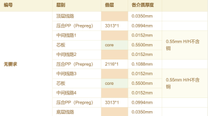
Table 1: Basic Structure of a 6 Layer PCB Stackup
| Layer Type | Description | Purpose |
|---|---|---|
| Signal Layer 1 | Outer layer for routing signals | Carry high-speed or sensitive signals |
| Ground Plane | Inner layer to provide a stable reference ground | Reduces noise and interference |
| Power Plane | Inner layer dedicated to power distribution | Supplies power to components |
| Signal Layer 2 | Another layer for routing signals | Provides additional routing space |
| Signal Layer 3 | Another layer for high-speed signal transmission | Supports high-frequency circuits |
| Outer Signal Layer | Final outer layer for routing signals | Final signal transmission layer |
2. What Makes a 6 Layer PCB Stackup Different?
The unique features of a 6 layer PCB stackup arise from the addition of more layers compared to simpler PCB designs. This enhanced structure allows for more complex routing and improved performance. Ready for the good part? The increased number of layers gives designers more flexibility in routing high-speed signals and distributing power efficiently, making it ideal for applications such as telecommunications, networking, and automotive electronics.
A 6 layer PCB stackup is especially beneficial for circuits that require high-speed signal transmission. The extra layers provide additional ground and power planes, which improve signal integrity by minimizing noise and providing a low-resistance path for the power supply. This structure also helps to prevent crosstalk between signal traces, a common issue in high-density designs.
The use of multiple signal layers also allows designers to maximize component placement efficiency, which is critical in applications where space is limited. Multi-layer stackups like the 6 layer design also provide better thermal management since the power and ground planes help dissipate heat more effectively.
Table 2: Advantages of a 6 Layer PCB Stackup
| Advantage | Description | Application |
|---|---|---|
| Improved Signal Integrity | Reduced noise and crosstalk by using dedicated signal layers | High-frequency circuits, RF applications |
| Enhanced Power Distribution | More ground and power planes for efficient power delivery | Automotive, aerospace |
| Compact Design | More routing space in fewer layers | Consumer electronics, wearables |
| Better Thermal Management | Improved heat dissipation through multiple planes | High-power applications |
3. Components of a 6 Layer PCB Stackup
A 6 layer PCB stackup consists of several key components that work together to provide high-performance, reliable electrical connections. Let’s break it down: each layer in a 6 layer PCB serves a distinct purpose. The signal layers handle the routing of electrical signals, while the power and ground planes ensure consistent power distribution and minimize noise.
The top and bottom layers, known as outer signal layers, are used to route signals that are connected to external components. These are typically high-frequency signals that require precise routing. The inner signal layers are used for additional signal routing, which is especially important for densely packed designs. Between these signal layers, the power and ground planes are used to provide stable voltage and reduce electromagnetic interference (EMI).
Additionally, isolation layers are used to separate signals and ensure they do not interfere with each other. These layers are critical for ensuring that high-speed signals maintain their integrity without degradation. Power distribution layers also play an essential role in minimizing power loss and ensuring that components receive the necessary voltage for proper operation.
Table 3: Breakdown of a 6 Layer PCB Stackup
| Layer Number | Type | Function |
|---|---|---|
| 1 | Outer Signal Layer | Routing high-speed or sensitive signals |
| 2 | Ground Plane | Provides stable reference ground |
| 3 | Power Plane | Distributes power to components |
| 4 | Inner Signal Layer | Additional signal routing |
| 5 | Inner Signal Layer | High-frequency signal routing |
| 6 | Outer Signal Layer | Final layer for routing signals |
4. Design Considerations for 6 Layer PCBs
Designing a 6 layer PCB requires careful planning and consideration of several factors, including layer stackup and impedance control. Ready for the good part? The added complexity of the 6 layer PCB means that designers must take into account not only the physical layer arrangement but also how the signal integrity, power distribution, and thermal properties of the board will perform under real-world conditions.
One of the most critical design considerations for 6 layer PCBs is impedance control. In high-speed digital circuits, controlling the impedance of traces ensures that signals are transmitted without distortion or loss of data. Additionally, ground and power planes must be carefully designed to ensure that the PCB can handle the power demands of the components while maintaining a low-noise environment.
When designing for a 6 layer stackup, thermal management is another important factor. Power components generate heat, and having efficient heat dissipation through proper layer stackup can ensure that the PCB remains functional even under high-load conditions. Designers often rely on thermal vias to carry heat away from critical areas to the ground plane or the outer layers.
Table 4: Key Design Considerations for 6 Layer PCBs
| Consideration | Description | Impact on PCB Performance |
|---|---|---|
| Impedance Control | Ensuring that the trace impedance matches the application requirements | Reduces signal reflection and data loss |
| Ground and Power Planes | Proper distribution of ground and power planes | Minimizes noise, ensures reliable power supply |
| Thermal Management | Efficient dissipation of heat from power components | Prevents overheating and failure of components |
| Trace Width & Spacing | Optimizing trace width and spacing for signal integrity | Ensures reliable signal transmission |
5. Applications of 6 Layer PCBs
6 layer PCBs are used in applications that require high-density routing and reliable signal integrity. What’s the real story? These PCBs are widely used in industries such as telecommunications, automotive, consumer electronics, and aerospace, where high-performance and compact designs are essential.
In telecommunications, 6 layer PCBs are used in base stations, routers, and satellite communication devices, where high-speed data transfer is critical. The multiple signal layers and power planes allow these boards to support high-frequency signals without degradation, ensuring reliable communication.
In the automotive industry, 6 layer PCBs are often found in advanced driver-assistance systems (ADAS), infotainment systems, and electric vehicle (EV) control units. These PCBs ensure that components perform reliably even under extreme temperature conditions and vibrations.
Additionally, consumer electronics like smartphones, smartwatches, and gaming consoles also benefit from 6 layer PCBs due to the need for compact designs with robust electrical performance.
Table 5: Common Applications of 6 Layer PCBs
| Industry | Application | Key Features |
|---|---|---|
| Telecommunications | Base stations, routers, communication devices | High-frequency signal routing, reliability |
| Automotive | ADAS, EV control units, infotainment systems | High performance, thermal management |
| Consumer Electronics | Smartphones, smartwatches, gaming consoles | Compact design, high-speed signal processing |
| Aerospace | Navigation systems, satellite electronics | Durability under extreme conditions |
6. Cost Considerations for 6 Layer PCBs
While 6 layer PCBs offer numerous advantages, they come at a higher cost compared to simpler 2-layer or 4-layer PCBs. But here’s the kicker: the increased cost is justified for applications requiring high performance, such as in telecommunications or high-end electronics.
The cost of a 6 layer PCB depends on various factors, including the complexity of the design, the materials used, and the manufacturing processes. For instance, high-frequency materials and advanced fabrication techniques can drive up costs. However, the increased performance and reliability provided by a 6 layer PCB often outweigh the additional expenses, particularly for industries where performance is critical.
Table 6: Cost Comparison of Different PCB Layer Configurations
| Layer Count | Estimated Cost Range | Application Type |
|---|---|---|
| 2 Layer PCB | Low | Simple consumer electronics |
| 4 Layer PCB | Moderate | Mid-range consumer electronics, automotive |
| 6 Layer PCB | High | High-performance electronics, telecommunications |
7. The Future of 6 Layer PCB Stackups
What’s the real story? The future of 6 layer PCBs looks promising, with innovations in materials and manufacturing processes continuing to expand their capabilities. Emerging trends like flexible PCBs, high-density interconnects (HDI), and 3D-printed PCBs are pushing the boundaries of what’s possible with multi-layer PCB designs.
As 5G technology and the Internet of Things (IoT) continue to evolve, the demand for faster, smaller, and more reliable electronics will drive the need for advanced stackups like the 6 layer PCB. Additionally, developments in automated PCB manufacturing and material science will continue to reduce costs and improve the performance of 6 layer designs, making them more accessible across various industries.
Table 7: Future Trends in 6 Layer PCB Stackups
| Trend | Description | Impact on PCB Industry |
|---|---|---|
| Flexible PCBs | Increasing demand for flexible, bendable PCBs | Enables more compact and durable designs |
| HDI and Microvia | Smaller vias and higher density interconnects | Pushes the limits of miniaturization |
| 3D-Printed PCBs | Additive manufacturing for custom designs | Reduces lead times, offers greater design flexibility |
| 5G and IoT Integration | Need for faster, more reliable circuits | Drives demand for advanced PCB stackups |
8. Conclusion: Why 6 Layer PCBs Are Essential for Modern Electronics
In conclusion, 6 layer PCBs are a vital component in the design and manufacturing of high-performance electronics. Ready for the kicker? Their unique ability to handle high-speed signals, provide reliable power distribution, and offer efficient thermal management makes them indispensable for industries like telecommunications, automotive, and aerospace. As technology continues to advance, 6 layer PCBs will play an even more critical role in enabling the next generation of electronic devices, providing designers with the tools they need to push the limits of what’s possible.
9. Manufacturing Challenges with 6 Layer PCBs
Manufacturing 6 layer PCBs comes with its own set of challenges. Ready for the kicker? Despite their many advantages, these boards are more difficult to fabricate than their simpler counterparts, and the increased complexity can lead to potential issues during production. Understanding these challenges can help mitigate potential issues and improve overall manufacturing efficiency.
One of the biggest challenges in 6 layer PCB manufacturing is drilling. Since 6 layer PCBs require multiple layers and vias, the drilling process is more intricate compared to simpler PCBs. Blind vias and buried vias need to be accurately drilled and plated to ensure reliable electrical connections between layers. Misalignment of the vias can result in significant defects, leading to increased scrap rates.
Additionally, layer alignment is a critical aspect of manufacturing 6 layer PCBs. Since multiple layers are stacked together, ensuring proper alignment during lamination is essential for maintaining electrical integrity. Misaligned layers can cause issues like open circuits or signal degradation.
The material selection for the different layers also adds to the complexity. Different materials may be required for the signal layers and power/ground planes, and maintaining uniform thickness across all layers is crucial for consistent performance. The manufacturing process must ensure that the material properties are maintained throughout the production cycle.
Table 8: Challenges in Manufacturing 6 Layer PCBs
| Challenge | Description | Solution |
|---|---|---|
| Drilling | Accurate drilling of vias in multiple layers | Use advanced drilling techniques, ensure precision |
| Layer Alignment | Maintaining alignment of all layers during lamination | Implement automated inspection systems |
| Material Selection | Selecting appropriate materials for each layer | Use high-quality materials with consistent properties |
| Plating and Vias | Plating vias and ensuring reliable electrical connection | Employ advanced plating techniques and quality control measures |
10. High-Speed Design Considerations for 6 Layer PCBs
High-speed circuits require a design approach that minimizes signal degradation, ensuring that data travels quickly and accurately across the PCB. What’s the real story? A 6 layer PCB stackup is ideal for high-speed applications because the extra layers provide the necessary separation and shielding to maintain signal integrity. Let’s explore the key design considerations for high-speed 6 layer PCBs.
One important aspect is impedance control. In high-speed designs, the impedance of traces must be controlled to ensure that signals are transmitted without reflections. The proper arrangement of signal, ground, and power planes in a 6 layer stackup helps to maintain the desired impedance throughout the entire PCB.
Signal integrity is another critical factor in high-speed PCB design. The distance between signal traces and the surrounding ground and power planes can affect the quality of the signal. To minimize crosstalk and electromagnetic interference (EMI), careful routing of signal traces and careful planning of the PCB stackup is essential.
Thermal management also plays a key role in high-speed designs. Power components on high-speed PCBs generate heat, and this heat can affect the performance of the circuits if not properly managed. A 6 layer PCB stackup provides additional layers for heat dissipation and can incorporate thermal vias that help carry heat away from critical components.
Table 9: High-Speed Design Considerations for 6 Layer PCBs
| Consideration | Description | Impact on High-Speed Design |
|---|---|---|
| Impedance Control | Ensuring that trace impedance is maintained | Minimizes signal reflections, ensures proper data transmission |
| Signal Integrity | Routing signal traces and maintaining ground separation | Prevents crosstalk and signal degradation |
| Thermal Management | Managing heat dissipation from power components | Ensures stable operation and prevents performance issues |
11. Testing and Quality Control for 6 Layer PCBs
To ensure that 6 layer PCBs perform reliably in demanding applications, thorough testing and quality control are essential. Ready for the good part? 6 layer PCBs require rigorous testing procedures to verify that they meet electrical, mechanical, and thermal requirements before they are used in final products.
In-circuit testing (ICT) is one of the most common methods used for testing 6 layer PCBs. This type of test checks for shorts, opens, and proper component placement by directly probing the PCB’s electrical points. ICT is an efficient way to detect faults early in the production process and ensure that the PCB meets design specifications.
Another essential test is visual inspection. Despite its simplicity, visual inspection can catch many manufacturing defects, such as misaligned layers, soldering issues, and component placement problems. Automated optical inspection (AOI) systems can provide a more detailed and consistent inspection than manual methods.
For high-frequency applications, high-speed testing is required to check the performance of the signal traces and ensure that the PCB can handle high-frequency data transmission without signal loss or interference. Additionally, thermal cycling tests simulate temperature variations to test the board’s reliability under changing environmental conditions.
Table 10: Common Testing Methods for 6 Layer PCBs
| Testing Method | Description | Benefit |
|---|---|---|
| In-Circuit Testing | Direct electrical testing to check for faults | Quickly detects shorts, opens, and incorrect components |
| Visual Inspection | Automated or manual inspection of the PCB | Identifies defects like misaligned layers and soldering issues |
| High-Speed Testing | Tests the integrity of high-frequency signals | Ensures reliable data transmission and signal integrity |
| Thermal Cycling | Testing PCB performance under temperature variations | Verifies reliability under temperature fluctuations |
12. Cost Considerations for 6 Layer PCBs
Cost is always a critical factor when designing PCBs. But here’s the kicker: while 6 layer PCBs come with higher manufacturing costs than simpler 2 or 4 layer designs, they are often necessary for high-performance applications. Understanding how the costs are structured can help you make informed decisions about whether a 6 layer stackup is the right choice for your product.
The material costs for 6 layer PCBs are generally higher because of the more complex construction and the need for multiple layers of conductive and insulating materials. Additionally, advanced manufacturing techniques such as laser drilling and automated placement of components can increase costs. However, the increased performance and capabilities of 6 layer PCBs often justify the added expense.
When evaluating costs, production volume is also an important factor. High-volume orders can help reduce the cost per unit, as the fixed costs associated with tooling and setup are spread across many units. For low-volume, custom, or prototype runs, however, the cost per unit may be significantly higher.
Table 11: Cost Breakdown of 6 Layer PCB Manufacturing
| Factor | Description | Impact on Cost |
|---|---|---|
| Material Costs | Use of high-quality materials for multiple layers | Increases production cost |
| Manufacturing Complexity | Use of advanced equipment for drilling and layer alignment | Adds to the overall cost |
| Production Volume | Larger production runs reduce per-unit cost | High-volume orders help lower unit cost |
| Testing and Quality Control | Rigorous testing and quality inspection | Essential for ensuring reliability but adds to cost |
13. How to Optimize 6 Layer PCB Stackups
Optimizing a 6 layer PCB stackup involves balancing multiple factors to ensure the board performs reliably while minimizing costs. Ready for the good part? Proper stackup design can enhance the PCB’s signal integrity, power distribution, and heat management without significantly increasing manufacturing costs.
Layer order is one of the most critical factors in optimizing a 6 layer PCB stackup. The optimal layer stackup depends on the specific requirements of the circuit. For example, placing power and ground planes close to signal layers helps ensure low impedance and reduces noise. Additionally, maintaining proper layer-to-layer distance ensures that the signal layers are sufficiently isolated from the power and ground planes to avoid crosstalk.
Trace width and spacing are also important in stackup optimization. Designers need to ensure that trace widths are appropriate for the current-carrying requirements of each signal, as well as to maintain consistent impedance across the entire PCB. Adjusting trace width and spacing helps improve signal integrity and power distribution.
Finally, thermal vias should be incorporated to help dissipate heat from high-power components. This is especially important in applications where components generate a significant amount of heat, such as power supplies or high-frequency circuits.
Table 12: Tips for Optimizing 6 Layer PCB Stackups
| Design Tip | Description | Benefit |
|---|---|---|
| Layer Order | Properly arrange signal, power, and ground planes | Optimizes signal integrity and reduces noise |
| Trace Width & Spacing | Ensure traces are sized appropriately for signal and current requirements | Improves reliability and reduces signal loss |
| Thermal Management | Include thermal vias to dissipate heat | Prevents overheating and ensures component longevity |
14. The Future of 6 Layer PCB Technology
The future of 6 layer PCBs looks bright as technology continues to evolve. What’s the real story? As the demand for smaller, faster, and more powerful devices increases, 6 layer PCBs will continue to play a crucial role in enabling these advancements. Future trends in 6 layer PCB technology include innovations in materials, manufacturing techniques, and design capabilities.
One exciting trend is the increased integration of flexible PCBs. Flexible 6 layer PCBs are expected to become more prevalent in wearable technology, medical devices, and even consumer electronics, where compactness and flexibility are critical. As 3D printing technologies improve, additive manufacturing will likely become more common in PCB production, allowing for custom, high-density designs with reduced lead times.
In addition, advancements in material science are paving the way for even higher-performance PCBs. Researchers are exploring materials that offer better electrical conductivity, higher thermal stability, and improved mechanical strength, all of which will benefit 6 layer PCB designs.
Table 13: Future Trends in 6 Layer PCB Technology
| Trend | Description | Impact on PCB Industry |
|---|---|---|
| Flexible PCBs | Increasing demand for flexible and bendable PCBs | Ideal for wearables and compact electronics |
| Additive Manufacturing | 3D printing and additive manufacturing methods | Reduces production time and cost |
| Advanced Materials | Use of high-performance materials for improved conductivity and strength | Improves overall PCB performance |
15. Conclusion: The Importance of 6 Layer PCBs
In conclusion, 6 layer PCBs are essential for modern electronic designs that demand high performance, reliability, and compactness. Ready for the kicker? Their ability to support high-speed signals, optimize power distribution, and manage thermal loads makes them indispensable in industries like telecommunications, aerospace, and automotive. As demand for more advanced electronics continues to rise, 6 layer PCBs will play an increasingly important role in enabling the next generation of devices.
FAQ Section
Q1: What is a 6 layer PCB stackup?
A1: A 6 layer PCB stackup consists of six layers of conductive and insulating materials arranged to create high-performance printed circuit boards. The stackup typically includes signal layers, power and ground planes, and isolation layers.
Q2: How does a 6 layer PCB stackup improve signal integrity?
A2: A 6 layer PCB stackup improves signal integrity by providing dedicated power and ground planes that reduce noise, minimize crosstalk, and maintain consistent impedance, especially in high-frequency applications.
Q3: What industries use 6 layer PCBs?
A3: 6 layer PCBs are used in telecommunications, automotive, aerospace, consumer electronics, and high-performance electronic devices where compact design and reliable signal transmission are essential.
Q4: What are the manufacturing challenges with 6 layer PCBs?
A4: Manufacturing challenges for 6 layer PCBs include precise drilling for vias, layer alignment during lamination, and material selection for each layer. These complexities require advanced equipment and techniques.
Q5: How do I optimize a 6 layer PCB stackup?
A5: To optimize a 6 layer PCB stackup, ensure proper layer order, maintain appropriate trace width and spacing for signal integrity, and incorporate thermal vias for heat dissipation, ensuring a high-performance and reliable design.

- long board pcb
- Flexible PCBs
- Special PCB
- Express Printed Circuit Board
- Pcb Prototype
- LED PCB
- PCB
- Printed Circuit Board
- Pcb meaning
- Pcb manufacturer
- Rigid pcb board
- Rigid Flex PCB
 Quote
Quote
 E-mail