PCB vias are essential components in the world of printed circuit boards (PCBs). These small yet crucial features play a significant role in ensuring that different layers of a PCB can communicate with each other electrically. In this article, we will explore the different types of PCB vias, their functions, how to design them efficiently, and the best practices for ensuring their optimal performance in your PCB designs.
PCB Vias
1. What Is a PCB Via?
A PCB via is a conductive hole that connects different layers of a printed circuit board. It allows for electrical signals to pass from one layer to another, making multi-layer PCB designs possible. Vias are necessary because they provide the pathways for signals to travel between various layers, and without them, the performance and functionality of multi-layered boards would be significantly compromised.
But here’s the kicker: PCB vias are not just holes—they are critical to the performance and manufacturability of your PCB. Each via type comes with its own design and manufacturing considerations, and the wrong choice could lead to poor performance or increased production costs. Essentially, vias help build the backbone of complex PCB designs, facilitating signal routing and thermal management.
Vias are typically filled with copper, making them conductive, and they are usually plated to ensure a reliable electrical connection. Understanding how vias work, and their impact on the overall design, is essential for any PCB designer.
Table 1: Key Components of PCB Vias
| Component | Description | Function |
|---|---|---|
| Via Hole | A hole drilled through the PCB layers | Allows electrical signals to pass between layers |
| Copper Fill | Copper material used to fill the via | Ensures reliable electrical connection |
| Via Plating | Plating that coats the via hole | Improves conductivity and provides structural integrity |
2. Types of PCB Vias
There are several types of PCB vias, each with its own application, advantages, and limitations. Understanding the different types of vias is crucial when designing PCBs, as each type serves a specific purpose and comes with design trade-offs.
What’s the real story? The choice of via type can significantly affect the performance, reliability, and cost of the final product. Let’s break down the four main types of PCB vias:
- Through-Hole Vias: These are the most common type of vias, where a hole is drilled all the way through the PCB, connecting the top and bottom layers. They are ideal for high-volume production and can handle high current but take up more space on the board.
- Blind Vias: These vias connect an outer layer to one or more inner layers but do not go through the entire board. Blind vias are typically used in designs where space is a concern and where routing needs to be confined to certain layers.
- Buried Vias: Unlike blind vias, buried vias only connect inner layers of the PCB. They do not have any connection to the outer layers of the board. These vias are used in designs that need to save space while still providing the necessary electrical connections.
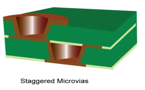
- Microvias: As the name suggests, microvias are very small vias typically used in high-density interconnect (HDI) PCBs. They allow for more compact designs and are commonly used in mobile devices, wearables, and other miniaturized products.
Table 2: Comparison of Different Types of PCB Vias
| Via Type | Description | Common Applications |
|---|---|---|
| Through-Hole Vias | Vias that go all the way through the PCB | High-volume production, standard PCBs |
| Blind Vias | Vias that connect outer layers to inner layers | High-density designs, space-constrained boards |
| Buried Vias | Vias that connect only inner layers | Complex multilayer designs, high-density boards |
| Microvias | Very small vias used for high-density designs | Wearables, mobile devices, HDI boards |
3. Functions of PCB Vias
The primary function of PCB vias is to enable electrical connections between different layers of a printed circuit board. However, their role goes beyond just electrical connectivity. Vias are also crucial for managing heat dissipation, controlling signal integrity, and facilitating the overall design of multi-layer PCBs.
This is where it gets interesting: vias allow designers to create multi-layered PCBs that are compact, high-performance, and efficient. They provide a way to route signals, power, and ground connections through different layers, enabling the design of more complex and powerful electronic devices. Vias are also integral to the thermal management of PCBs, allowing heat to be dissipated efficiently from high-power components.
- Electrical Connection: The most basic function of vias is to establish a conductive path between layers, enabling the flow of signals or power across different PCB layers.
- Signal Routing: Vias allow signal paths to travel vertically through the PCB, which is crucial for high-density designs where horizontal space is limited.
- Thermal Management: Vias are used to create pathways for heat to flow away from heat-sensitive components, thus helping to maintain the optimal temperature of the PCB.
Table 3: Functions of PCB Vias
| Function | Description | Impact on PCB Design |
|---|---|---|
| Electrical Connection | Connects different PCB layers electrically | Enables signal and power transmission between layers |
| Signal Routing | Directs signal flow through the PCB | Facilitates routing in complex designs |
| Thermal Management | Helps dissipate heat from components | Improves performance and reliability by managing temperature |
4. How PCB Vias Are Manufactured
The manufacturing of PCB vias involves several precise steps to ensure proper functionality. These steps include drilling, plating, and finishing, all of which contribute to the final performance of the vias.
Ready for the good part? The process starts with drilling a hole in the PCB, followed by the deposition of a thin copper layer to make the hole conductive. The via is then plated with copper to form a solid electrical connection. After plating, the vias are typically cleaned, and sometimes filled with materials to improve their strength or conductivity.
- Drilling: The first step in via creation is drilling the hole in the PCB. This is usually done using a laser or mechanical drill.
- Plating: Once the hole is drilled, copper is plated onto the walls of the via, making it electrically conductive.
- Finishing: The via is then finished with additional treatments, such as via filling or plugging, depending on the application.
Table 4: Steps in PCB Via Manufacturing
| Step | Description | Purpose |
|---|---|---|
| Drilling | Hole is drilled through the PCB layers | Creates a path for electrical connection |
| Plating | Copper is plated onto the walls of the via | Makes the via electrically conductive |
| Finishing | Via is filled or plugged if needed | Enhances via strength and electrical properties |
5. The Role of Vias in Multilayer PCBs
Multilayer PCBs are designed to support complex electronic circuits that need to fit into a small footprint. Vias play a crucial role in these designs, as they provide the necessary connections between the layers of the PCB. Without vias, the performance and reliability of multilayer PCBs would be significantly compromised.
What’s the real story? Vias are the enablers of multi-layered designs, allowing for compact, high-performance PCBs that power everything from consumer electronics to automotive systems. In multilayer PCBs, vias facilitate the routing of signals, ground planes, and power distribution, ensuring that each layer can function independently while still communicating with the others. The use of vias allows designers to maximize space and performance in tightly packed designs.
Table 5: Importance of Vias in Multilayer PCBs
| Role | Description | Impact on Design |
|---|---|---|
| Signal Routing | Vias help route signals between PCB layers | Ensures that all layers are properly connected |
| Power Distribution | Vias distribute power across the PCB | Essential for delivering power to different sections of the PCB |
| Space Optimization | Vias reduce the need for external connections | Maximizes space efficiency in complex designs |
6. Design Considerations for PCB Vias
When designing PCB vias, several considerations must be taken into account to ensure they are effective and cost-efficient. These include via size, placement, and the overall layout of the PCB.
But here’s the kicker: Designing vias is not just about making holes—it’s about ensuring that each via is optimized for electrical performance, manufacturability, and cost-effectiveness. Small changes in via design can lead to significant improvements in signal integrity and production efficiency. Here are some key factors to consider when designing vias:
- Via Size: The size of the via directly impacts its cost, performance, and manufacturability. Smaller vias are often used in high-density designs but require more precise manufacturing techniques.
- Via Placement: The placement of vias is crucial for ensuring that signals and power are routed efficiently. Poor placement can lead to signal interference or inefficient use of space.
- Via Aspect Ratio: This is the ratio between the via’s length and diameter, and it affects the via’s strength and reliability.
Table 6: Design Considerations for PCB Vias
| Consideration | Description | Impact on Design |
|---|---|---|
| Via Size | The diameter of the via | Affects manufacturability, performance, and cost |
| Via Placement | Positioning of the via on the PCB | Ensures efficient routing and minimizes interference |
| Via Aspect Ratio | The ratio between via length and diameter | Impacts via strength, reliability, and cost |
7. Via Fill and Via Plugging
Via fill and via plugging are two techniques used to enhance the functionality and reliability of vias in a PCB design. These techniques are particularly useful for improving the performance of high-frequency PCBs and ensuring that vias do not cause issues with signal integrity.
Ready for the good part? Via filling involves filling the via with a conductive material, which can improve the thermal and electrical performance of the via. Via plugging, on the other hand, involves filling the via with a non-conductive material, effectively preventing it from being part of the electrical circuit. These methods are commonly used in high-density interconnect (HDI) boards or when vias are placed near sensitive components that require optimal performance.
Table 7: Via Fill vs. Via Plugging
| Technique | Description | Purpose |
|---|---|---|
| Via Fill | The via is filled with a conductive material | Improves thermal and electrical performance |
| Via Plugging | The via is filled with a non-conductive material | Prevents electrical connectivity in specific vias |
8. Via Impedance and Signal Integrity
Impedance matching is essential for ensuring that signals travel through vias without distortion or loss. Improper via design can cause impedance mismatches, leading to signal reflections and integrity issues.
This is where it gets interesting: Via impedance can be controlled by adjusting the size of the via, the materials used, and the placement within the PCB layout. Ensuring that the via impedance matches the characteristic impedance of the PCB traces is crucial for maintaining high-speed signal integrity. Signal integrity issues caused by vias can lead to data errors, reduced performance, and system failures, making it essential to manage via impedance properly in your designs.
Table 8: Via Impedance vs. Signal Integrity
| Factor | Description | Impact on Signal Integrity |
|---|---|---|
| Via Size | The diameter of the via | Affects impedance and signal quality |
| Via Material | The material used to fill the via | Impacts conductivity and signal loss |
| Via Placement | Positioning of vias relative to traces | Ensures proper impedance matching for signals |
9. Best Practices for PCB Via Design
Ensuring the optimal performance of vias requires adherence to best practices throughout the design and manufacturing processes. From selecting the right via type to ensuring proper placement, these practices help avoid costly mistakes and design flaws.
What’s the real story? By following these best practices, you can optimize the electrical performance of your PCBs, improve manufacturability, and minimize production costs. Here are the top practices to follow for efficient via design:
- Select the Right Via Type: Understand the application and choose the correct via type (through-hole, blind, buried, or microvia) based on your needs.
- Ensure Proper Via Size and Placement: Optimize via size and placement to reduce signal interference and increase routing efficiency.
- Use Proper Via Impedance Matching: Ensure that via impedance matches the signal traces to maintain signal integrity.
Table 9: Best Practices for PCB Via Design
| Best Practice | Description | Benefit |
|---|---|---|
| Choose the Right Via Type | Select the appropriate via type based on application | Ensures efficient routing and electrical performance |
| Optimize Via Size | Properly size vias to minimize space and ensure performance | Reduces PCB size and improves manufacturability |
| Match Via Impedance | Ensure impedance matching between vias and traces | Prevents signal reflection and integrity issues |
10. Conclusion
PCB vias are integral to the functionality and manufacturability of multi-layered circuit boards. Understanding the different types of vias, their functions, and how to design them effectively can significantly improve PCB performance, reduce costs, and streamline the production process. Whether dealing with signal integrity, thermal management, or routing efficiency, proper via design is crucial for creating high-performance PCBs.
FAQ
Q1: What is a PCB via?
A PCB via is a conductive hole in a PCB that connects different layers, allowing signals and power to pass between them.
Q2: How are PCB vias manufactured?
PCB vias are manufactured by drilling holes into the PCB, plating the holes with copper to make them conductive, and sometimes filling or plugging them for specific purposes.
Q3: What are the different types of PCB vias?
The main types of PCB vias are through-hole, blind, buried, and microvias, each with specific applications and benefits.
Q4: Why is impedance matching important for PCB vias?
Impedance matching ensures that signals travel through vias without distortion, preventing data errors and performance issues.
Q5: How can I optimize my PCB via design?
Optimize via design by selecting the appropriate via type, ensuring proper size and placement, and matching impedance to maintain signal integrity and improve manufacturability.

- long board pcb
- Flexible PCBs
- Special PCB
- Express Printed Circuit Board
- Pcb Prototype
- LED PCB
- PCB
- Printed Circuit Board
- Pcb meaning
- Pcb manufacturer
- Rigid pcb board
- Rigid Flex PCB
 Quote
Quote
 E-mail