1. Introduction to Castellated PCB
In the realm of printed circuit board (PCB) technologies, Castellated PCB has emerged as a transformative innovation, especially in modular integration and microelectronic applications. These unique boards are defined by their scalloped or half-hole edges, which enable seamless soldering to another PCB surface, essentially turning the PCB itself into a solderable module. This feature allows manufacturers to create reusable, stackable, or plugin sub-systems with improved connectivity and minimized component duplication.
Castellation, by definition, refers to the series of half-holes (or vias cut in half) along the edge of a PCB. These plated-through holes are often aligned with precise spacing to allow interconnection between two circuit boards, much like how pins on a traditional chip module might be soldered to a mother board. This makes Castellated PCB a popular choice for breakout boards, sensor modules, communication chips, and RF devices.
The concept is simple in principle but powerful in its implications. By enabling a PCB to serve as both a substrate and a connector, it reduces the need for additional interface components. For example, a Wi-Fi module with castellations can be directly soldered onto a baseboard without needing sockets, headers, or extensive wiring.
Despite its niche use case compared to standard PCBs, Castellated PCB has witnessed increasing adoption across industries such as consumer electronics, automotive, aerospace, medical devices, and Internet of Things (IoT). Its appeal lies not only in the space-saving layout but also in the cost-effectiveness and ease of integration it offers when scaling modular electronics.
As someone who has worked extensively with modular PCB systems, I find castellated designs particularly valuable when developing reusable blocks for embedded systems. The ability to build, test, and iterate small modules before full integration speeds up prototyping. It also aids in fault isolation during the debugging phase, since a problematic module can simply be de-soldered and replaced with minimal disruption.
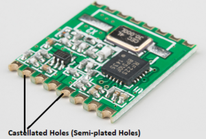
Castellated PCB
2. Historical Development of Castellated PCB
The Castellated PCB has not always been a mainstream element of circuit design, but its historical development reflects the broader evolution of modular electronics and surface-mount technologies. Understanding where castellated edges came from requires a brief overview of how interconnect strategies have matured over time.
◾ From Wire-Wrapped Boards to Modular PCBs
In the early days of electronics, wiring was done manually, often using wire-wrap or point-to-point soldering. These methods, while functional, were bulky and prone to reliability issues. As the electronics industry shifted toward mass production, printed circuit boards became the norm due to their reproducibility and compact size.
The rise of modular design began in earnest with the development of components like plug-in daughterboards and multi-layer PCBs. The modular approach allowed designers to create reusable functional units—microprocessor modules, communication interfaces, or sensor hubs—that could be plugged into larger systems. However, traditional methods of interconnecting modules often relied on pin headers, sockets, or edge connectors, all of which added height, cost, and complexity.
It was during this phase that Castellated PCB emerged as an alternative interconnect method—one that enabled a PCB to mimic the behavior of a surface-mount component.
◾ Birth of Castellated Designs
The castellated edge, sometimes referred to historically as a “scalloped via pattern” or “half-hole PCB,” came into more common use in the 1990s, particularly with the miniaturization of wireless communication modules. The method allowed one PCB to be surface-soldered to another, saving vertical space and reducing the need for mechanical connectors.
This innovation closely paralleled the advent of surface-mount device (SMD) packaging. As manufacturers moved away from through-hole components to reduce size and improve automation, the idea of making PCBs behave like SMDs gained traction. A Castellated PCB became, effectively, a large, flat electronic component with built-in pads along its edge.
One of the earliest widespread applications was in RF modules. Small PCBs containing Bluetooth, Zigbee, or Wi-Fi radios were equipped with castellated holes so they could be soldered directly to host PCBs without sacrificing space. This trend significantly reduced manufacturing costs and enabled more streamlined design processes.
◾ Evolution with IoT and Embedded Systems
In the 2000s and beyond, the explosion of embedded systems, especially in consumer electronics and IoT devices, accelerated the adoption of Castellated PCB. Modules such as GPS units, environmental sensors, or microcontroller boards became widely available with castellated designs. These were often offered as breakout boards for developers and engineers needing rapid integration with host systems.
The popularity of development platforms like Arduino and Raspberry Pi also played a role. Many third-party hardware vendors began producing castellated add-ons to be mounted on baseboards, allowing advanced functionalities like GSM communication, LoRa transmission, or analog-to-digital conversion to be modularized.
From an engineer’s perspective, the increasing reliability of this interconnect method made it more than just a prototype solution. Castellated modules are now trusted in production-grade devices, especially when pin count is low and signal speed is manageable.
◾ Manufacturing Advances
The evolution of Castellated PCB also mirrored improvements in PCB fabrication. In the past, routing plated-through holes exactly on the edge of a board posed a challenge, especially when maintaining consistent plating integrity. Over time, as CNC milling and laser cutting technologies advanced, board shops were able to consistently produce clean, plated half-holes with repeatable results.
This made it easier for designers to specify castellated edges in their Gerber files, knowing that manufacturers could reliably deliver boards that passed both visual and electrical inspection. Today, nearly all major PCB fabs support this feature, and some even have standard guidelines and templates for it.
◾ Personal Reflection
Looking back, I believe the true value of Castellated PCB lies in its democratizing effect. It bridged the gap between surface-mount design and modular prototyping. As someone who started with traditional header-based integration, I was initially cautious about castellated modules due to concerns about soldering strength and inspection. But after deploying several castellated solutions in compact wireless designs and observing their reliability in field applications, I now consider it an essential tool in the modular electronics toolkit.
3. Structural Characteristics of Castellated PCB
The structural design of a Castellated PCB is what sets it apart from conventional printed circuit boards. The unique layout and machining technique involved in creating the castellated, or half-hole, edges provides both electrical and mechanical benefits. A detailed examination of these characteristics reveals why this structure is favored in modular and embedded system designs.
◾ What Defines a Castellated Structure?
At its core, a Castellated PCB features plated through-holes that are partially removed at the edge of the board. These holes—originally drilled like standard vias—are later routed in such a way that they are cut exactly in half during the final milling or profiling stage of PCB fabrication.
The result is a series of semi-circular or scallop-shaped openings, often evenly spaced along one or more edges of the PCB. These are fully plated internally, maintaining electrical continuity between top and bottom layers and ensuring that they can be soldered directly to matching pads on a base PCB.
This configuration essentially turns the edge of the PCB into a series of accessible pins or contact points. Just as a quad flat no-lead (QFN) package uses edge pads to surface-mount a chip, a Castellated PCB uses these plated half-holes to mount one board onto another.
◾ Standard Design Parameters
While there are no absolute universal standards for castellated via placement, several guidelines have become widely adopted among designers and manufacturers:
-
Hole diameter: Usually between 0.4 mm to 0.8 mm.
-
Hole spacing (pitch): Generally 1.27 mm (50 mil) or 2.54 mm (100 mil), depending on the application.
-
Annular ring width: Often kept at 0.1 mm to 0.15 mm to ensure reliable plating.
-
Edge clearance: A minimal distance between the edge of the board and the center of the via is required to ensure manufacturability, typically around 0.25 mm or more.
The exact dimensions depend on the complexity of the design, the signal integrity requirements, and the capabilities of the PCB fabrication facility. For high-density interconnect (HDI) applications, smaller via diameters and tighter spacing can be used, but this raises the bar for manufacturing precision.
◾ Layer Considerations in Castellated PCB
In multi-layer designs, Castellated PCB structures typically involve vias that traverse all layers, allowing consistent interconnection from top to bottom. This ensures that signals or power routed through inner layers can reach the base PCB without additional jumpers or vias.
However, special attention must be paid to how internal traces terminate at the castellated vias. For example, high-speed signals may require impedance-controlled traces that transition smoothly through the edge connections, which complicates the design.
Also, solder mask reliefs must be carefully defined to expose the plated edges without overexposing adjacent pads or traces. In some designs, a solder mask dam is placed between the castellated hole and internal copper pours to reduce the risk of solder bridging.
◾ Mechanical and Thermal Stability
A major structural advantage of the Castellated PCB is its relatively strong mechanical attachment to the host board. When properly soldered, the scalloped edges provide a stable interface with good tensile strength. Still, because the solder joint is primarily at the edge rather than embedded like a through-hole pin, vibration resistance is lower than traditional connectors unless additional reinforcement is applied.
Thermal characteristics also come into play. Castellated holes—being plated—conduct heat efficiently, which can aid in thermal dissipation. However, designers must ensure that excessive thermal gradients do not lead to stress cracking or delamination at the edge during reflow or wave soldering processes.
From a reliability perspective, thermal fatigue resistance can be enhanced by maintaining consistent pad-to-hole ratios, using symmetrical layer stack-ups, and ensuring precise alignment between the castellated PCB and the baseboard.
◾ My Observations from Prototyping
In my own experience, the structural simplicity of the Castellated PCB is both its biggest strength and its potential weakness. On one hand, it removes the need for separate connectors or complicated pin headers. On the other hand, the margin for soldering error is narrow. If the castellated pads do not align perfectly with the base PCB, or if solder paste application is inconsistent, the resulting joint can be weak or even electrically open.
That said, when proper design rules are followed and manufacturer capabilities are matched, the structural integrity is more than sufficient even in environments with moderate mechanical stress. For instance, I once deployed a castellated microcontroller module in a handheld device subject to frequent handling. After more than a year in use, there was no degradation in signal quality or structural bond.
Ultimately, a well-structured Castellated PCB must be a product of both good engineering design and disciplined manufacturing practices. It’s a fusion of electrical precision and mechanical foresight.
4. Design Considerations for Castellated PCB
Designing a Castellated PCB involves a nuanced balance between electrical performance, mechanical strength, manufacturability, and functional integration. Unlike conventional PCBs, which rely on internal routing and standard via placement, castellated structures introduce edge-based connectivity that affects the entire design process—from layout and pad geometry to assembly strategies and signal integrity.
In this section, we explore the key parameters and best practices that PCB designers must consider when developing a board with castellated features.
◾ Pad Alignment and Via Placement Strategy
One of the first considerations when creating a Castellated PCB is the precise alignment of the castellated vias along the PCB edge. These vias should ideally be positioned symmetrically to distribute mechanical and electrical loads evenly. Misaligned or unevenly spaced vias can create issues during both the soldering process and electrical inspection.
Common guidelines include:
-
Consistent spacing: Choose a pitch that corresponds to the pad layout of the base PCB (e.g., 1.27mm for many embedded modules).
-
Even distribution: Avoid clustering vias near corners or unsupported areas.
-
Via center-to-edge distance: Ensure the via centers are located precisely along the board edge to ensure half-via exposure during milling.
Good alignment isn’t just about aesthetics—it directly impacts soldering quality and electrical contact during surface mounting.
◾ Electrical Considerations in Castellated PCB Design
When designing a Castellated PCB, one must treat the edge vias as critical interconnection nodes. These are not mere mechanical anchors; they carry power, ground, data, and clock signals. Therefore, their electrical properties must be considered carefully.
Key practices include:
-
Controlled impedance traces: For high-speed or RF applications, the routing to castellated pads should follow impedance-matching rules, especially when connecting to transmission lines on the host PCB.
-
Short trace lengths: Keep connections between internal components and edge vias as short and direct as possible to reduce inductance and signal delay.
-
Minimize stubs: Unused or open-ended vias near the board edge should be removed or terminated to avoid reflection in high-frequency signals.
-
Separate analog and digital domains: If both analog and digital signals pass through castellated edges, their placement and return path strategies must be isolated and carefully managed.
These techniques help ensure signal fidelity and reduce the chance of cross-talk, noise, or impedance mismatch at the module’s edge.
◾ Solder Mask, Paste Mask, and Silkscreen Management
A crucial yet often overlooked design aspect of the Castellated PCB is proper definition of solder mask and paste mask layers. Since castellated vias serve as surface-mount points, ensuring clean pad exposure is essential for proper soldering.
Recommendations include:
-
Solder mask clearance: Ensure solder mask is pulled back sufficiently around each castellated via to avoid incomplete soldering or bridging.
-
Paste mask apertures: If the board will be reflow soldered onto a base PCB, define appropriate stencil openings for solder paste deposition.
-
Avoid silkscreen overlap: Text or marking near castellated edges should be kept away to avoid interference with soldering or automated optical inspection (AOI).
Some designers choose to leave the entire castellated edge free of any solder mask, relying solely on surface tension to wick solder correctly into the plated half-hole. This depends heavily on the quality of board fabrication and soldering process used.
◾ Mechanical Mounting and Board Shape Constraints
When planning the mechanical interface of a Castellated PCB, several physical constraints must be addressed:
-
Edge clearance: Ensure sufficient space around the castellated edge for a soldering iron tip or reflow nozzle, especially if manual rework is anticipated.
-
Corner rounding: Sharp corners near the castellated vias should be avoided. Rounded or chamfered corners reduce mechanical stress and prevent delamination.
-
Depanelization method: The choice of V-score vs. tab-routing affects how cleanly castellated edges are formed during final board separation. Careless depaneling can crack or deform the half-vias.
Moreover, when integrating with a host PCB, designers must account for component placement on both the top and bottom sides. Components too close to the castellated edge may interfere with soldering or increase the chance of thermal shadowing during reflow.
◾ Design for Manufacturability (DFM)
Working closely with the PCB fabricator is critical during Castellated PCB design. While most modern PCB fabs support half-via routing, tolerances and process limitations vary. DFM guidelines ensure higher yield and lower defect rates.
Some DFM-oriented suggestions include:
-
Use standard via sizes that fall within the manufacturer’s tooling range.
-
Specify castellated regions explicitly in fabrication drawings, preferably with a note or layer in the Gerber file.
-
Confirm plating integrity—request cross-section or X-ray inspection reports if the board is part of a mission-critical system.
-
Communicate edge tolerance requirements for clean, symmetrical cuts through vias.
As someone who has experienced both smooth and problematic builds, I strongly recommend involving the fabricator early in the design phase. A small oversight in via size, edge clearance, or stack-up asymmetry can lead to poor yield and costly rework.
◾ Personal Thoughts on Design Trade-offs
In my view, the elegance of the Castellated PCB lies in its dual nature—it is both a circuit and a connector. But this dual role demands higher attention to design discipline. While it simplifies integration, it also exposes the edge of the PCB to more mechanical and environmental stress.
For mission-critical applications, I usually complement castellated edge connections with adhesive underfill or mechanical clips. For cost-sensitive consumer devices, I accept the risk but increase inspection rigor. Like many advanced design features, castellated edges are not a silver bullet—they require thoughtful planning, iterative testing, and precise execution.
5. Fabrication Techniques of Castellated PCB
The fabrication of a Castellated PCB introduces unique challenges compared to conventional board production. Creating half-plated holes precisely at the edge of a PCB requires advanced routing, reliable through-hole plating, and strict adherence to geometric tolerances. A well-manufactured castellated edge must maintain electrical continuity, mechanical robustness, and visual symmetry—all while conforming to the demands of modern surface-mount assembly.
Let us break down the major steps, technologies, and quality controls involved in fabricating such a board.
◾ Standard Manufacturing Flow for Castellated PCB
The general PCB fabrication process remains mostly intact when producing a Castellated PCB, but additional steps are introduced during and after the drilling phase.
-
Drilling of Through-Holes:
Standard via holes are drilled through the board at specified positions along what will eventually be the edge. These holes are planned to be cut in half later. -
Through-Hole Plating:
A copper plating process (electroless followed by electrolytic deposition) is used to plate the inner walls of these drilled holes. For castellations, high-quality plating is critical, as the structural integrity of the final solder joint depends on this plating being exposed cleanly at the edge. -
Image Transfer and Etching:
Standard photolithography is used to define the circuit traces. The copper is etched to form pads, traces, and other features, including the ring around each castellated via. -
Solder Mask and Silkscreen:
A solder mask is applied to prevent accidental bridging and oxidation. Areas around the castellated edges are typically left open or precisely masked to ensure clean exposure of the plated walls. -
Routing or Milling (Edge Profiling):
This is the defining step for a Castellated PCB. A CNC router or mechanical mill cuts through the already plated vias, splitting them cleanly in half and creating the “castellated” edge. Precision is essential to ensure a symmetric cross-section and prevent burrs or delamination. -
Surface Finish Application:
Finishes such as ENIG (Electroless Nickel Immersion Gold), HASL (Hot Air Solder Leveling), or OSP (Organic Solderability Preservatives) are applied. For castellated holes, ENIG is often preferred because it coats both the surface and the exposed walls consistently. -
Electrical and Optical Testing:
Electrical continuity testing ensures that all castellated connections are intact. Visual inspections and sometimes X-ray imaging are used to verify plating uniformity and cut-edge quality.
◾ Precision Challenges in Milling and Plating
One of the most critical fabrication aspects of a Castellated PCB lies in the accuracy of the milling process. The router must pass exactly through the centerline of the via. Any deviation—whether due to tool drift, wear, or setup misalignment—can result in:
-
Asymmetrical half-holes
-
Exposed fiberglass instead of plated copper
-
Poor solderability on the base PCB
-
Mechanical weaknesses during vibration or thermal cycling
To counter these issues, reputable PCB manufacturers use CNC machines with micron-level repeatability and rigid quality controls. Some even opt for laser-assisted profiling for ultra-fine applications.
Likewise, plating must be uniform across the board, especially around vias scheduled for edge cutting. Uneven plating can lead to incomplete copper coverage on the exposed walls, which not only affects conductivity but can cause solder wetting problems.
◾ Design-for-Fabrication (DFF) Tips
Designers intending to fabricate a Castellated PCB should follow specific DFF principles to ease the manufacturing process and enhance output quality:
-
Avoid blind vias at the edge—always use through-holes to simplify plating.
-
Maintain minimum wall thickness of 0.25 mm around half-holes to preserve structural integrity.
-
Cluster half-holes on a single edge where possible to reduce milling complexity.
-
Communicate intent with explicit fabrication notes indicating which vias are to be castellation-processed.
Providing manufacturers with a “castellation drawing” or a special mechanical layer marking castellated areas can dramatically reduce miscommunication and scrap rate.
◾ Surface Finish Selection and Solderability
Choosing the correct surface finish is essential for Castellated PCB performance. Since the edge of the via is directly involved in soldering, the finish must promote excellent wetting and oxidation resistance.
-
ENIG (Electroless Nickel Immersion Gold):
Offers excellent surface flatness, corrosion resistance, and strong solderability. Preferred for castellated modules, especially in RF or gold-contact applications. -
HASL (Hot Air Solder Leveling):
Cost-effective but may result in uneven pad heights, which is problematic for castellated pads. -
OSP (Organic Solderability Preservatives):
Works well in lead-free processes but may degrade over time, especially at exposed edges.
I’ve personally found that ENIG provides the most consistent results across varying humidity and thermal environments. Though slightly more expensive, it minimizes solder defects during module attachment and ensures long-term reliability.
◾ Inspection and Quality Assurance for Castellated PCB
Because Castellated PCB features are often used in high-reliability applications (e.g., wireless modules, sensor interfaces), rigorous inspection is critical.
-
AOI (Automated Optical Inspection):
Checks for solder mask misalignment, via ovality, and registration errors. -
Electrical Continuity Testing:
Ensures internal connections from the castellated pad to inner layers are valid. -
X-ray Imaging:
Optional but highly effective in verifying via wall plating and edge integrity, especially for complex multilayer boards.
If a module fails inspection due to improper castellation, rework is rarely possible—it is usually scrapped. This makes first-pass fabrication accuracy extremely important.
◾ My Practical Experience with Fabrication Partners
From my own experience working with several board manufacturers across China, Europe, and North America, I’ve seen a wide variance in the quality of Castellated PCB outputs. Some low-cost fabs offer castellation but use basic mechanical routers with poor edge alignment, resulting in rough or uneven half-holes. Others specialize in RF modules and provide polished, gold-plated castellated edges with X-ray-certified plating.
When reliability is paramount, I recommend requesting samples or prototype runs first. Once you identify a capable fabrication partner who consistently delivers clean castellated features, build a long-term relationship—they’re worth it.
6. Materials Used in Castellated PCB Manufacturing
The material selection for a Castellated PCB plays a vital role in determining not only the electrical and thermal performance of the board but also the quality of the castellation itself. Unlike generic circuit boards, where edges remain non-functional, a castellated structure transforms part of the board’s edge into an active interconnection interface. This added functionality imposes stricter demands on the materials used throughout the stack-up and finishing processes.
In this section, we explore the types of materials typically used in Castellated PCB production, how they affect manufacturability and performance, and what trade-offs designers must consider when choosing them.
◾ Base Substrate Materials for Castellated PCB
At the heart of any PCB lies its substrate—the dielectric material that provides mechanical support and electrical insulation. For Castellated PCB, the substrate must support precise milling, resist thermal expansion, and maintain plating adhesion at cut edges.
Common substrates include:
-
FR-4 (Flame Retardant-4):
The industry standard for most PCBs, FR-4 is a fiberglass-reinforced epoxy laminate that offers excellent dimensional stability, electrical insulation, and mechanical strength. It is widely used for castellated designs, especially in consumer electronics and IoT applications. -
High-Tg FR-4:
For applications exposed to higher operating temperatures or more frequent thermal cycling, a high glass transition temperature (Tg) FR-4 improves reliability. This is important for castellated structures that undergo multiple soldering cycles. -
Rogers or Teflon-based substrates:
In RF and microwave applications, where Castellated PCB modules are commonly used, low-loss dielectric materials like Rogers (e.g., RO4003C) or PTFE composites may be preferred. These substrates offer superior signal integrity but require specialized fabrication techniques. -
Polyimide or Flexible Laminates:
Used rarely for castellated designs due to complexity, but in multilayer hybrid boards combining rigid and flex regions, polyimide’s thermal stability can be advantageous.
When selecting a substrate for castellated boards, one must also consider the ability of the material to survive edge milling without delaminating or splintering. Not all materials respond well to post-plating mechanical stress, which makes FR-4 the most balanced and widely adopted option.
◾ Copper Foil and Conductive Layers
A Castellated PCB relies heavily on the quality and consistency of its copper layers—particularly in and around the vias destined to be cut in half.
Important copper characteristics include:
-
Thickness:
Typical outer copper thickness ranges from 1 oz/ft² (35 µm) to 2 oz/ft² (70 µm). Thicker copper layers are used for power modules or boards carrying significant current. However, thicker copper complicates fine-pitch milling at the castellated edge. -
Adhesion:
Strong copper-substrate adhesion is critical. If copper delaminates during routing or thermal stress, castellated edges may lose electrical continuity or experience solder lift-off. -
Uniformity:
Variations in copper thickness can lead to uneven plating within vias and inconsistent edge exposure. For castellated structures, any irregularity becomes immediately visible and problematic.
For high-reliability designs, I recommend specifying IPC Class 2 or Class 3 copper layer tolerances in fabrication documentation. This helps ensure better plating results in the final castellated cuts.
◾ Via Wall Plating Materials
The strength and conductivity of the Castellated PCB‘s connection depends on the plating quality of the through-hole walls that are later exposed. These plated edges act as electrical contacts and solder anchors.
Standard materials include:
-
Electroless Copper:
Forms the initial plating layer inside the via holes. It ensures complete coverage before electrolytic copper is deposited. -
Electrolytic Copper:
Builds up the thickness of the via wall plating. Ideal plating thickness is typically 20–25 µm for good mechanical durability, especially when the via will be cut in half. -
Optional: Nickel and Gold (ENIG):
ENIG is often used as a surface finish but also coats the exposed walls of the castellated via if applied after routing. This offers additional corrosion resistance and enhances solderability.
Careful control of the plating process ensures that the exposed edges of the vias remain conductive and robust under both reflow and long-term use.
◾ Surface Finishing Materials
The final surface finish applied to a Castellated PCB determines solderability and corrosion resistance. Since castellated pads are surface-mounted, the surface finish must be uniformly applied across both planar and vertically exposed via edges.
Common finishing materials include:
-
ENIG (Electroless Nickel Immersion Gold):
A preferred choice for castellated edges due to its smooth surface, long shelf life, and excellent solderability. It also enhances visual inspection, especially under AOI systems. -
Immersion Tin or Silver:
Cheaper alternatives to ENIG, these finishes provide good solderability but are more sensitive to oxidation and shelf-life issues. -
HASL (Hot Air Solder Leveling):
While economical, HASL may not coat the vertical walls of castellated vias uniformly, leading to unpredictable soldering behavior. It’s generally discouraged for precision applications. -
OSP (Organic Solderability Preservatives):
Environmentally friendly and cost-effective but unsuitable for castellated vias that will be stored long-term or exposed to multiple solder cycles.
In my personal prototyping work, I’ve had the most consistent results with ENIG finishes—especially when dealing with modules meant for production-level soldering to a mainboard. The added cost is easily justified by the reduction in rework and improved solder joint reliability.
◾ My Perspective on Material Optimization
From experience, I find the material decisions for a Castellated PCB come down to balancing mechanical precision with thermal and electrical demands. For example, if you’re building a high-frequency LoRa or Wi-Fi module, using Rogers material and ENIG finish with tightly controlled copper thickness delivers excellent signal integrity. But for a simple sensor module targeting cost-sensitive markets, FR-4 with standard copper and immersion silver may be sufficient.
It’s critical to avoid over-engineering. Over-specifying materials can drive up costs with little functional gain, while under-specifying may result in board failure at the solder joint or signal integrity problems.
Always match your material choices to the application context and longevity expectations of your product.
7. Castellated PCB in Modular Electronics
The evolution of modular electronics has significantly reshaped how modern electronic systems are designed, prototyped, and deployed. At the heart of this shift lies the demand for compact, reconfigurable, and scalable circuit designs. Within this landscape, the Castellated PCB has become an indispensable element—acting as both a functional sub-circuit and an interconnect interface.
In this section, we explore how Castellated PCB contributes to modular electronic design, why it’s preferred in certain architectures, and how it enables design reuse, faster prototyping, and efficient mass production.
◾ The Role of Castellated PCB in Modular Architecture
Modular electronics refers to the practice of dividing a complex system into smaller, self-contained units or modules that can be developed, tested, and replaced independently. This design philosophy emphasizes flexibility, scalability, and rapid development.
The Castellated PCB fits perfectly into this paradigm because it:
-
Acts as a drop-in module that can be surface-soldered to a host PCB.
-
Eliminates the need for bulky connectors or headers that add cost and height.
-
Allows reusability and interchangeability, enabling engineers to swap or upgrade functionality without altering the base design.
-
Reduces wire clutter and improves mechanical stability by being soldered directly to the motherboard.
This is especially valuable in environments like development boards, sensor platforms, RF modules, and power regulators, where multiple modules are designed to plug into a shared base system.
◾ Use Cases and Examples in Modular Design
1. Wireless Communication Modules:
Many Wi-Fi, Bluetooth, Zigbee, and LoRa modules come in Castellated PCB format. This allows them to be integrated into any host board with minimal space overhead. For example, the ESP32 or nRF52840 modules are popular castellated boards in IoT development.
2. Breakout Boards:
In prototyping environments, castellated PCBs are used to create breakout boards for fine-pitch or complex ICs. These boards convert BGA or QFN components into a more accessible layout, enabling engineers to work with them on a breadboard or larger system without specialized reflow equipment.
3. Power Supply Modules:
Buck/boost converters, battery charging circuits, and voltage regulators are often implemented as castellated PCBs to facilitate plug-and-play power distribution in embedded platforms.
4. Microcontroller Subsystems:
Miniature MCUs (like STM32F0 or ATmega328 modules) are often embedded on castellated PCBs. This isolates critical functions from the mainboard and accelerates debugging or iteration without redesigning the whole product.
◾ Advantages Over Traditional Interconnects
Compared to traditional headers, sockets, or edge connectors, Castellated PCB offers several benefits:
-
Lower profile and space saving:
Ideal for slim designs such as wearables and handheld devices. -
Cost efficiency in volume production:
Eliminates need for male/female headers and associated assembly steps. -
Improved electrical performance:
Shorter path lengths and cleaner signal integrity due to direct soldering. -
Enhanced mechanical rigidity:
When properly soldered, castellated joints are surprisingly strong and less prone to vibration-related fatigue than pin-based systems.
However, castellated modules are typically not designed for frequent removal or reuse. Unlike socketed modules, they are semi-permanently mounted and may not suit every modular system—especially where field upgradability is a requirement.
◾ My Reflections on Real-World Modular Projects
In my own work, I’ve deployed Castellated PCB modules in both hobbyist and commercial projects. One example involved designing a modular sensing platform for agricultural monitoring. Each sensor type (soil moisture, light, CO₂, temperature) was implemented as a castellated module. The baseboard handled power, I²C communication, and data aggregation.
This approach allowed us to develop, test, and manufacture sensors in parallel, then integrate them selectively based on customer requirements. The result was not only a faster time-to-market but also a more customizable product line.
Another project focused on integrating castellated ESP32 communication modules into a smart lighting system. The castellated form factor allowed for easy soldering to the mainboard, but more importantly, made field repairs practical. Damaged or outdated modules could be de-soldered and replaced without affecting the rest of the system—a huge benefit in installations with hundreds of devices.
8. Advantages of Using Castellated PCB
The Castellated PCB has earned widespread recognition for its unique combination of simplicity, compactness, and functionality. Whether in consumer electronics, industrial systems, or rapid prototyping environments, castellated designs empower engineers and manufacturers to achieve tighter integration with fewer components.
In this section, we will outline the primary benefits of adopting Castellated PCB in product development and electronic system design, highlighting both technical merits and commercial implications.
◾ 1. Compact Form Factor for Space-Constrained Designs
A major advantage of the Castellated PCB lies in its ability to minimize space usage without sacrificing functionality. By embedding the edge interconnects directly into the module, it eliminates the need for bulky headers, sockets, or mezzanine connectors.
This compactness offers particular value in:
-
Wearables and portable devices where thickness and board area are tightly constrained.
-
Smart sensors that must be embedded in tight enclosures, such as those in smart homes, agriculture, or asset tracking.
-
Densely populated systems where vertical clearance must be minimized, such as drones and IoT edge devices.
Because castellated modules function like surface-mount devices (SMDs), they align well with other low-profile components, enabling streamlined mechanical design.
◾ 2. Cost-Effective Integration
Cost reduction is another key benefit of using a Castellated PCB. By eliminating connectors, the total bill of materials (BOM) is significantly reduced—not only in terms of component cost, but also in terms of:
-
Assembly time
-
Testing complexity
-
Mechanical support structures
In high-volume manufacturing, every component counts. Castellated modules simplify the pick-and-place process by allowing the module to be treated as a single SMD component. This accelerates SMT line efficiency and reduces post-assembly handling.
Moreover, castellated modules can often be sourced from third-party suppliers as pre-certified functional blocks (e.g., Wi-Fi modules), further reducing certification, RF layout, and firmware development costs.
◾ 3. Faster Time to Market
For startups, R&D teams, and prototyping environments, the Castellated PCB offers a fast track from concept to working prototype. Designers can purchase or build modular sub-circuits, solder them onto a baseboard, and begin testing functionality almost immediately.
This has a direct impact on:
-
Prototype iteration cycles
-
Development velocity
-
Minimum viable product (MVP) rollout
In my experience, castellated modules have cut development time by as much as 40% for complex systems. For example, integrating an existing BLE module as a castellated PCB allowed us to bypass all RF design, antenna tuning, and compliance work—and focus on application-layer development.
◾ 4. Enhanced System Reliability
When implemented correctly, a Castellated PCB offers strong and reliable interconnection. While not as robust as through-hole pin headers in extreme mechanical conditions, properly soldered castellated pads deliver:
-
Low resistance, low-inductance connections
-
Excellent thermal conductivity across the solder joint
-
High signal integrity, especially in low-speed or moderate-speed buses (e.g., I²C, UART, SPI)
This makes them particularly suitable for embedded systems that are factory-assembled and sealed, where the module will not be removed during service life.
Additionally, eliminating mechanical connectors reduces the potential for issues like:
-
Connector fatigue
-
Oxidation or corrosion of contacts
-
Assembly errors due to pin misalignment
◾ 5. Ideal for Pre-Certified and Plug-and-Play Modules
Many regulatory and compliance-heavy systems—especially those with RF or wireless functions—benefit from pre-certified modules. These modules are often packaged as Castellated PCBs, making integration nearly effortless.
For instance:
-
FCC/CE-certified Wi-Fi or Bluetooth modules (e.g., ESP32-WROOM, RN4871)
-
GNSS/GPS receivers in castellated packages
-
MCU+radio combo modules for Zigbee, Thread, LoRa, or BLE
Using these certified modules avoids the need to re-verify emissions, RF layout performance, or safety compliance, accelerating the route to market while reducing risk and cost.
◾ 6. Simplified Debugging and Testing
Because castellated modules often expose all necessary signals at the edge, they make debugging and testing easier. Developers can probe castellated pads with:
-
Fine-pitch clip probes
-
Edge-mounted test jigs
-
Oscilloscopes or logic analyzers
This accessibility is especially useful during bring-up or hardware validation phases. Some designers even build test jigs specifically for castellated interfaces, enabling automated test coverage of the module before it’s integrated into the host PCB.
Conclusion
The Castellated PCB is a critical enabler of modular electronics, offering a balance of mechanical robustness and ease of assembly. As technology progresses, advancements in materials, manufacturing, and automation will further enhance its role in modern electronics. Engineers and designers must continue refining Castellated PCB techniques to meet the growing demands of miniaturization and high-performance applications.
My experience with Castellated PCB technology confirms its value as a versatile bridge between modularity and manufacturability. It elegantly balances the need for compactness and robust connection, especially in the rapidly expanding domains of IoT and wearable devices.
However, successful adoption hinges on a deep understanding of its constraints and the willingness to invest in precise design, fabrication, and assembly practices. Collaboration with experienced PCB fabricators and assembly houses is vital.
Looking forward, I am optimistic that emerging innovations—especially in materials science and AI-driven manufacturing—will continue to enhance castellated PCB technology, enabling even more compact, reliable, and multifunctional electronic systems.

- long board pcb
- Flexible PCBs
- Special PCB
- Express Printed Circuit Board
- Pcb Prototype
- LED PCB
- PCB
- Printed Circuit Board
- Pcb meaning
- Pcb manufacturer
- Rigid pcb board
- Rigid Flex PCB
 Quote
Quote
 E-mail