1. Introduction: Understanding Tenting Vias in PCB Manufacturing
In the intricate world of printed circuit board (PCB) design, the details matter. Every via, trace, and pad has a specific purpose that contributes to the functionality and reliability of an electronic device. Among these design features, tenting vias play a unique role in both electrical performance and mechanical protection. The process of tenting involves covering via holes with solder mask material—typically without filling the via completely—either to shield the vias from environmental contaminants or to optimize surface mount technology (SMT) processes. While this technique has existed for decades, its utility and practicality continue to be assessed and re-evaluated in light of technological advancements and evolving industry demands.
Tenting vias in PCB manufacturing is not simply about aesthetics or simplicity; it has practical implications for signal integrity, manufacturability, reliability, and even cost. It represents a trade-off between ease of production and long-term functionality, making it a topic of ongoing interest and debate among designers and engineers.
In recent years, new technologies and fabrication processes have emerged, offering alternatives to traditional tenting methods. These innovations challenge conventional practices and provide new solutions for managing vias, especially in high-density and high-frequency designs. As such, understanding the advantages, limitations, and potential replacements for tenting vias has become essential for anyone involved in PCB layout, assembly, or quality assurance.
This article explores the many facets of tenting vias in PCB manufacturing. It begins with foundational knowledge, offering a historical perspective and technical overview. Then, it delves into the materials and manufacturing processes involved, before moving on to a detailed analysis of the pros and cons of the method. Alternatives such as via plugging, via filling, and via-in-pad will also be examined, with comparative analysis highlighting scenarios where one approach may be preferred over another.
Importantly, this article is not just a recitation of facts. It includes critical reflections and professional insights gathered from real-world experience in PCB design and fabrication. It aims to balance theoretical understanding with practical considerations, providing the reader with the tools to make informed decisions.
In a rapidly evolving industry where performance expectations continue to rise, and the margin for error shrinks, a deep understanding of tenting vias in PCB manufacturing—and the possible alternatives—can make the difference between a successful product launch and a costly design failure.
Tenting Vias in PCB manufacturing
2. Basic Concepts Behind Tenting Vias in PCB Manufacturing
To fully understand the implications and relevance of tenting vias in PCB manufacturing, it’s crucial to begin with the fundamental concepts behind this technique. At its core, tenting refers to the process of covering via holes—small drilled holes that connect different layers of a PCB—with solder mask material during the fabrication process. The aim is to protect the via from contamination, mechanical damage, or unintended solder bridging during the assembly stage.
2.1 What Is a Via?
A via (short for “Vertical Interconnect Access”) is a conductive pathway that allows electrical connections between different layers of a PCB. Vias are drilled through the board and then plated with copper to ensure continuity. Depending on the board’s complexity, vias can be categorized as:
-
Through-hole vias: These go all the way from the top layer to the bottom layer.
-
Blind vias: These connect outer layers to one or more inner layers without penetrating the entire board.
-
Buried vias: These exist entirely within internal layers and are not visible on the outer surfaces.
Tenting can be applied to any of these via types, though it is most commonly associated with through-hole vias on simpler or double-sided boards.
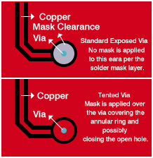
2.2 What Is Tenting?
In PCB manufacturing, tenting refers to applying a solder mask layer over the via to form a “tent” that covers the opening. There are two common forms of tenting:
-
Partial tenting: The solder mask covers the via pad, but the via hole remains open or partially covered.
-
Full tenting: The solder mask completely covers the via and hole, ideally forming a sealed protective barrier.
Tenting differs from other methods such as plugging (where vias are filled with a non-conductive material) and via-in-pad (where vias are placed directly under SMT pads and usually filled and capped).
2.3 Why Use Tenting?
There are several primary motivations behind using tenting vias in PCB manufacturing:
-
Protection from Contamination: Solder mask over vias prevents solder, flux, and other contaminants from entering the via hole, which could lead to shorts or corrosion.
-
Improved Soldering Results: Tenting can reduce solder bridging between via holes and adjacent pads, especially in fine-pitch SMT designs.
-
Mechanical Protection: Tented vias are less prone to damage from probing, handling, or environmental stress.
-
Aesthetic Improvement: Fully tented vias provide a cleaner board appearance, which is beneficial in consumer electronics.
2.4 Key Factors Affecting Tenting
Several variables influence the success of tenting vias in PCB manufacturing:
-
Via Size: Smaller vias (typically <0.3 mm) are easier to tent fully with solder mask, whereas larger vias may require additional processing.
-
Solder Mask Type and Thickness: The viscosity and curing properties of the solder mask determine how well it can cover the via without forming voids or bubbles.
-
Board Layout: Dense or complex layouts can make tenting more challenging due to spacing and alignment limitations.
-
Fabrication Tolerances: Manufacturing precision is key to achieving consistent tenting across all vias in the design.
Understanding these basic concepts is vital for engineers and designers, as it lays the groundwork for evaluating when tenting vias in PCB manufacturing is beneficial and when alternative methods might be more appropriate.
3. Historical Development of Tenting Vias in PCB Manufacturing
To appreciate the current landscape and future direction of tenting vias in PCB manufacturing, it’s helpful to trace how this practice has evolved over time. From its roots in early PCB designs to its adaptation in high-density and high-frequency boards, tenting has undergone significant transformations shaped by technological progress, manufacturing capabilities, and the increasing complexity of electronic devices.
3.1 Early Adoption of Tenting Vias in PCB Manufacturing
In the early days of PCB production—during the 1960s and 1970s—via structures were relatively large and manufacturing processes were less precise than they are today. Vias were typically left open, as the risk of contamination or interference with soldering was minimal in simple through-hole assemblies. The need to tent vias arose only when boards began to shrink and surface mount technology (SMT) started gaining traction.
As surface mount components became more common in the 1980s, designers noticed that open vias posed problems such as:
-
Solder wicking, where solder would be drawn into the via hole, creating poor solder joints on component pads.
-
Bridging and shorts, especially between closely spaced pads and vias.
To address these issues, tenting vias with solder mask was introduced as a protective measure. Initially, tenting was achieved using standard screen printing methods for applying the solder mask, but this often resulted in inconsistent coverage and reliability.
3.2 Advancements in Solder Mask Application
The 1990s saw major improvements in solder mask materials and application techniques. Liquid Photoimageable Solder Mask (LPI) became the industry standard, allowing for:
-
Finer resolution
-
Improved alignment
-
Better adhesion to the board surface
-
Enhanced ability to tent smaller via holes
These improvements made it feasible to consistently tent vias under 0.5 mm in diameter, increasing the use of this method in compact and high-reliability designs.
With the increasing adoption of multilayer PCBs and complex routing, tenting became more of a design necessity. However, designers also encountered limitations, such as voids under the solder mask or masks cracking during thermal cycles. This prompted experimentation with alternative techniques like via plugging and via-in-pad.
3.3 The Role of Tenting Vias in HDI and High-Speed Boards
As High-Density Interconnect (HDI) boards became more prevalent in the early 2000s, the relevance of tenting vias in PCB manufacturing took on new dimensions. While tenting was still used for basic protection, its suitability for very small vias (microvias) came into question. HDI designs often use laser-drilled microvias with diameters below 0.2 mm, which are difficult to tent reliably using traditional methods.
At the same time, high-speed digital signals required better impedance control and lower signal reflections. Open vias introduced the risk of stubs and unwanted radiation, making tenting a less favorable solution. As a result, many high-speed boards shifted toward filled vias and back-drilling techniques, reducing the dominance of tenting in performance-critical applications.
3.4 Contemporary Use of Tenting Vias in PCB Manufacturing
Today, tenting vias remain a common practice, especially in:
-
Consumer electronics
-
Industrial control systems
-
Automotive PCBs with moderate complexity
-
Applications where cost is a greater concern than peak performance
However, manufacturers now offer hybrid approaches like tenting plus plugging, which combines the affordability of tenting with the reliability of via-filling for select parts of the design. Some advanced fabs also support vacuum-assisted solder mask application, improving the reliability of full tenting even on denser boards.
In conclusion, tenting vias in PCB manufacturing has matured from a niche protective technique into a mainstream design element that must be considered in relation to design goals, product environment, and manufacturing capabilities. Understanding its historical development helps highlight not only the strengths of this method but also its contextual limitations—paving the way for smarter choices and innovative alternatives.
4. Materials Used for Tenting Vias in PCB Manufacturing
The effectiveness of tenting vias in PCB manufacturing hinges largely on the materials used in the process. Proper material selection not only impacts the durability and protective performance of the tented vias but also affects downstream processes such as assembly, reflow soldering, and board longevity. This section explores the primary materials employed in tenting vias and evaluates their respective characteristics and trade-offs.
4.1 Solder Mask Materials for Tenting Vias in PCB Manufacturing
The most common material used for tenting vias is the solder mask, which acts as a protective barrier applied over the PCB surface. Solder masks are typically epoxy-based and come in different formulations depending on the application and manufacturing process. The most widely used solder mask types include:
4.1.1 Liquid Photoimageable (LPI) Solder Mask
-
Properties: LPI is a photosensitive, epoxy-based material applied in liquid form.
-
Application: Applied via silkscreen or curtain coating, then imaged and cured using UV exposure.
-
Advantages:
-
High resolution, suitable for fine-pitch designs.
-
Good adhesion to copper and laminate surfaces.
-
Cost-effective and widely supported in manufacturing.
-
-
Limitations:
-
May not fully cover larger vias or those in densely populated areas.
-
Susceptible to voiding or pinholing if improperly cured.
-
4.1.2 Dry Film Solder Mask (DFSM)
-
Properties: A solid film material that is laminated onto the board.
-
Application: Applied through a lamination process and exposed using photolithography.
-
Advantages:
-
Consistent thickness and better coverage over larger or irregular surfaces.
-
Excellent dielectric strength.
-
-
Limitations:
-
More expensive than LPI.
-
Less commonly used for tenting because of application complexity.
-
4.2 Specialized Inks and Coatings in Tenting Vias in PCB Manufacturing
Beyond conventional solder masks, specialized inks and coatings are sometimes employed for tenting vias, especially in environments requiring extra durability or environmental protection.
-
Thermally Curable Inks:
-
Offer high chemical resistance and mechanical strength.
-
Often used in automotive or aerospace applications.
-
-
UV Curable Coatings:
-
Provide rapid processing, suitable for high-throughput production.
-
May be prone to undercure in vias unless optimized carefully.
-
These materials offer unique performance profiles but are generally used in niche or high-end products where cost is less of a concern.
4.3 Adhesion and Compatibility Issues in Tenting Vias in PCB Manufacturing
One of the most critical factors in selecting a tenting material is its adhesion to both copper and laminate surfaces. Poor adhesion may lead to:
-
Delamination during thermal cycling.
-
Moisture ingress through micro-cracks in the solder mask.
-
Solder mask lifting, leading to potential exposure of vias during soldering.
To combat these issues, manufacturers often prepare the PCB surface with micro-etching or plasma cleaning prior to solder mask application.
In addition, compatibility with reflow profiles and chemical resistance during flux cleaning must be considered, especially in lead-free assembly processes, which tend to operate at higher temperatures.
4.4 Material Trade-offs in Tenting Vias in PCB Manufacturing
No single material offers a perfect solution for every application. Designers and manufacturers must weigh several trade-offs:
| Property | LPI Solder Mask | Dry Film | Specialty Inks |
|---|---|---|---|
| Cost | Low | High | Variable |
| Via Coverage | Moderate | High | High |
| Processing Speed | Fast | Slow | Medium |
| Durability | Moderate | High | High |
| Adhesion | Good | Very Good | Good |
In lower-cost consumer electronics, LPI remains the standard for tenting vias. For mission-critical boards, higher-end materials are more likely to be justified due to the need for increased performance and environmental resilience.
5. Design Considerations for Tenting Vias in PCB Manufacturing
When implementing tenting vias in PCB manufacturing, design decisions play a pivotal role in the long-term reliability, manufacturability, and cost-efficiency of the final product. This section examines critical design aspects that influence the success of tenting vias, and how layout engineers can strategically optimize their designs for better outcomes.
5.1 Via Size and Spacing in Tenting Vias in PCB Manufacturing
One of the primary design elements that affects tenting effectiveness is the diameter of the via and the clearance between adjacent vias or pads.
-
Smaller vias (typically < 0.3 mm) are easier to tent because the solder mask can fully cover and adhere to the top opening without collapsing into the hole.
-
Larger vias may result in incomplete coverage or mask breakage during curing or assembly.
-
Close spacing between vias may cause solder mask bridging, while too much spacing may leave more surface exposed, creating inconsistencies in the mask application.
Thus, an optimal balance must be achieved based on application needs and solder mask capabilities.
5.2 Pad and Via Relationship in Tenting Vias in PCB Manufacturing
Another essential aspect involves the spatial relationship between component pads and vias.
-
Vias placed directly under or near BGA pads (ball grid arrays) are particularly sensitive to solder bridging during reflow.
-
In such cases, tenting is highly recommended to prevent solder wicking into the via, which could cause cold joints or open circuits.
-
Designers often choose via-in-pad with tenting or via-in-pad with fill and cap plating to resolve this, depending on budget and performance needs.
5.3 Solder Mask Expansion Parameters for Tenting Vias in PCB Manufacturing
Proper solder mask expansion (or mask swell) around vias is crucial to ensuring reliable tenting:
-
If the expansion is too small, the solder mask may not adhere well to the copper ring, leading to delamination.
-
If the expansion is too large, unintended areas may be covered or exposed, affecting circuit performance.
-
Most design guidelines recommend a swell of 2 to 5 mils beyond the via diameter for optimal tenting performance.
Additionally, careful alignment during photolithography is necessary to prevent mask shifting, which can expose the via unintentionally.
5.4 Double-Sided Tenting Strategies in Tenting Vias in PCB Manufacturing
For more robust protection, double-sided tenting—applying solder mask to both top and bottom via openings—is a common strategy. However, it introduces its own challenges:
-
Pros:
-
Enhanced isolation from environmental factors.
-
Reduces the risk of solder ingress from either side.
-
-
Cons:
-
Increased processing complexity.
-
Greater risk of trapped air or incomplete mask coverage.
-
Designers must coordinate with manufacturers to determine whether double-sided tenting is viable and cost-justified for their specific application.
5.5 Thermal and Signal Integrity in Tenting Vias in PCB Manufacturing
Via tenting can impact both thermal dissipation and signal performance, especially in high-speed or high-frequency boards.
-
Thermally, a tented via reduces heat escape paths compared to an open via.
-
Electrically, tented vias may slightly affect impedance if they’re part of a transmission line structure, particularly if the via’s plating or shape is irregular due to mask interference.
To address these concerns, simulation tools such as thermal modeling and signal integrity analysis should be used during design validation.
6. Process of Applying Tenting Vias in PCB Manufacturing
The process of applying tenting vias in PCB manufacturing is more than simply covering holes with solder mask. It involves a series of tightly controlled fabrication steps, material selections, and inspection processes to ensure full via coverage and reliable long-term performance. In this section, we break down each stage of the tenting application process and highlight key technical factors that impact the result.
6.1 Solder Mask Material Selection in Tenting Vias in PCB Manufacturing
The process begins with choosing the right solder mask type—a crucial step that determines adhesion strength, thermal stability, and coverage capability.
-
Liquid Photoimageable Solder Mask (LPI): This is the industry standard due to its fine resolution and compatibility with tenting.
-
Dry Film Solder Mask (DFSM): Less common for tenting, but still used for specific design rules or military-grade applications.
-
Material must exhibit:
-
High resolution
-
Strong adhesion to copper
-
Good coverage on uneven surfaces
-
Minimal shrinkage after curing
-
The viscosity and flow properties of the mask material influence how effectively it will tent vias, especially in high-density designs.
6.2 Via Preparation and Cleaning for Tenting Vias in PCB Manufacturing
Before solder mask application, vias must be thoroughly cleaned to ensure strong adhesion and proper coverage:
-
Debris removal from drilling (resin smear, burrs)
-
Desmearing and plasma cleaning to improve surface energy
-
Surface roughening via microetch to aid solder mask bonding
Failure to prepare the via correctly can lead to solder mask lifting, incomplete tenting, or early failure during assembly.
6.3 Solder Mask Application in Tenting Vias in PCB Manufacturing
The solder mask is typically applied in a silkscreen or curtain coating process, followed by UV exposure to define the pattern.
-
Coating: A uniform layer of solder mask is applied over the entire panel, ensuring it flows into and over the vias.
-
Pre-baking: The panel is dried to a semi-cured state (also called “tack dry”) to hold the mask in place before exposure.
-
UV Exposure: A phototool with the solder mask pattern is used to expose the desired areas. Vias that are to be tented are masked off from exposure to remain unexposed and thus remain fully covered.
This process requires precise alignment, especially when tenting both sides of the board.
6.4 Development and Curing of Tenting Vias in PCB Manufacturing
After exposure, the PCB undergoes development and final curing:
-
Development: The panel is washed in an alkaline solution to remove unexposed areas. Vias that were covered in the non-exposed regions remain tented.
-
Inspection: Optical or AOI systems check for incomplete tenting, pinholes, or undercut.
-
Curing: The final hardening of the solder mask is done through thermal curing or UV curing, depending on the mask formulation.
Proper curing ensures chemical and mechanical durability of the solder mask during subsequent reflow, wave soldering, or thermal cycling.
6.5 Quality Control in Tenting Vias in PCB Manufacturing
Quality control is essential to verify that tenting vias meet design specifications and reliability standards:
-
Visual inspection: Looks for mask peeling, cracking, or missed vias.
-
Cross-sectional analysis: Occasionally used to confirm complete coverage on high-reliability boards.
-
Solderability tests: Ensure no unintended openings expose copper and cause solder bridging.
Documentation and traceability are important in regulated industries (aerospace, automotive) to ensure compliance with IPC and MIL standards.
7. Pros of Using Tenting Vias in PCB Manufacturing
The use of tenting vias in PCB manufacturing brings numerous benefits to both the manufacturing process and the overall performance and reliability of electronic assemblies. While not universally applicable, this technique offers specific advantages that make it a valuable option in a wide range of PCB designs. This section discusses the primary benefits of tenting vias, supported by technical rationale and real-world considerations.
7.1 Improved Protection of Via Holes in Tenting Vias in PCB Manufacturing
One of the most prominent advantages of tenting vias is the protection of via holes from external contaminants:
-
Moisture resistance: Prevents water ingress that could lead to corrosion or electrical leakage.
-
Dust and particle exclusion: Keeps debris out of small via holes, especially in dirty environments.
-
Chemical shielding: Helps protect copper via walls during flux or cleaning exposure.
This physical barrier enhances the durability of the PCB, especially in outdoor, automotive, or industrial applications.
7.2 Reduced Risk of Solder Bridging in Tenting Vias in PCB Manufacturing
Tenting vias helps prevent solder bridging during the assembly process, particularly when vias are located close to component pads:
-
Vias that are not tented may wick solder away from SMT pads, causing weak joints.
-
Uncovered vias can create unwanted solder connections between traces or components.
-
This makes tenting particularly valuable in fine-pitch BGA and QFN designs where spacing is tight.
By maintaining solder control, tenting contributes to higher yield rates and fewer rework issues.
7.3 Enhanced Electrical Performance in Tenting Vias in PCB Manufacturing
From an electrical standpoint, tented vias help maintain signal integrity by eliminating exposed metal surfaces:
-
Reduces the risk of EMI (Electromagnetic Interference) caused by open copper areas.
-
Helps maintain consistent impedance by ensuring uninterrupted solder mask over the surface.
-
Reduces the chance of crosstalk from unintended coupling through via holes in high-speed circuits.
These characteristics make tenting favorable in RF, high-frequency, and high-speed digital designs.
7.4 Aesthetic and Functional Surface Finish in Tenting Vias in PCB Manufacturing
Tenting vias contributes to a cleaner surface appearance, which has both visual and practical advantages:
-
Improves the surface flatness and uniformity of the board.
-
Supports better silkscreen legibility when vias are not disrupting text or markers.
-
Helps avoid conductive paste bleed in assembly steps like stencil printing.
In consumer products and presentation boards, this can also enhance perceived quality.
7.5 Cost-Effective Reliability Enhancement in Tenting Vias in PCB Manufacturing
Compared to more complex via protection methods (like via plugging or filling), tenting is cost-effective:
-
Uses standard solder mask application processes.
-
No need for additional equipment or processing steps.
-
Quick implementation in design rules with minimal layout changes.
Tenting provides a reliable protection method without significantly increasing board cost, making it ideal for mid-volume and price-sensitive projects.
7.6 Environmental and Mechanical Durability in Tenting Vias in PCB Manufacturing
Tenting contributes to the mechanical robustness of the PCB during and after fabrication:
-
Prevents via wall damage during handling and soldering.
-
Reduces the chance of delamination and mask cracking due to covered and stabilized features.
-
Protects vias from thermal stress in multiple reflow cycles.
Especially in ruggedized electronics (like military, automotive, or aerospace), these benefits are crucial to extending service life.
8. Cons of Using Tenting Vias in PCB Manufacturing
Despite its advantages, tenting vias is not a universal solution. There are several limitations and disadvantages that designers and manufacturers must take into account when considering this method. This section examines the key concerns and challenges associated with tenting vias in PCB manufacturing and how they may impact product reliability, performance, and production efficiency.
8.1 Incomplete Coverage Issues in Tenting Vias in PCB Manufacturing
One of the primary drawbacks of tenting vias is incomplete via coverage:
-
Solder mask gaps or pinholes may form over the via, exposing copper to environmental elements.
-
Poor alignment or uneven mask thickness can cause the mask to recede or lift, especially in large-diameter vias.
-
Inadequate sealing leaves vias vulnerable to moisture ingress and oxidation, undermining the protective purpose of tenting.
These inconsistencies can lead to field failures, especially in high-humidity or corrosive environments.
8.2 Voiding and Air Traps in Tenting Vias in PCB Manufacturing
Trapped air beneath the tented solder mask can create voids, resulting in:
-
Outgassing during soldering or reflow, which may damage the solder mask or nearby components.
-
Delamination or blistering if pressure builds up within the trapped cavity.
-
Long-term reliability issues due to thermal cycling effects on the sealed cavity.
Such outcomes are difficult to detect during visual inspection and can compromise product longevity.
8.3 Incompatibility with Certain Assembly Requirements in Tenting Vias in PCB Manufacturing
Tented vias can present obstacles in specific assembly conditions:
-
In via-in-pad designs, tenting alone is often insufficient to prevent solder wicking, leading to assembly defects.
-
Some applications require vacuum soldering or underfill, where sealed vias interfere with venting or adhesion.
-
Test pad accessibility is reduced when vias are covered, complicating electrical testing and in-circuit diagnostics.
These limitations must be carefully considered when integrating tenting with modern assembly processes.
8.4 Design Rule Constraints in Tenting Vias in PCB Manufacturing
Solder mask application imposes limitations on design freedom:
-
Minimum mask clearance rules may conflict with dense via arrays, particularly in HDI (High-Density Interconnect) boards.
-
Small via sizes may not receive effective mask coverage due to resolution limitations.
-
Designers may need to modify via placement or pad geometry, which can impact signal integrity or routing efficiency.
These compromises can reduce the efficiency of high-speed or compact layouts.
8.5 Mechanical and Thermal Stress Sensitivity in Tenting Vias in PCB Manufacturing
Tented vias can become stress points in the PCB, especially under harsh environmental conditions:
-
Thermal cycling can cause solder mask cracks or separation over time.
-
Mechanical flexing may lead to microcracks around the tented area, exposing copper and weakening connections.
-
If tenting is damaged during handling, it can expose the via to solder splash or corrosion.
These issues are particularly critical in military, aerospace, or automotive sectors where mechanical robustness is non-negotiable.
8.6 Inadequate for High-Reliability Applications in Tenting Vias in PCB Manufacturing
While tenting vias may suffice for many consumer and commercial applications, it often does not meet the standards required for mission-critical electronics:
-
Applications that demand void-free, gas-tight seals (such as medical or defense electronics) prefer via filling or capping methods.
-
IPC Class 3 boards often disallow tenting as a primary via protection method due to its variability.
-
Tenting may be seen as a low-cost compromise, unsuitable for systems that require complete reliability assurance.
Thus, it is essential to match the tenting strategy with the reliability class and end-use of the PCB.
9. Alternatives to Tenting Vias in PCB Manufacturing
While tenting vias is a widely used practice in PCB design, its limitations make it necessary to consider alternative via protection and sealing methods—especially in high-performance or high-reliability applications. In this section, we explore the most prevalent alternatives to tenting vias in PCB manufacturing, assessing their advantages, appropriate use cases, and implementation considerations.
9.1 Via Plugging as an Alternative to Tenting Vias in PCB Manufacturing
Via plugging involves filling the via hole—either partially or completely—with a non-conductive or conductive paste, followed by planarization:
-
Improves reliability by eliminating air pockets and preventing solder from wicking into the via.
-
Allows for via-in-pad designs, particularly in HDI applications.
-
Suitable for both through-hole and blind vias.
However, plugging increases process complexity and cost. Proper paste curing and surface finishing are critical to avoid reliability concerns.
9.2 Via Filling with Copper in Place of Tenting Vias in PCB Manufacturing
Copper filling is a premium method where the via is filled with electroplated copper:
-
Provides maximum mechanical strength and thermal conductivity.
-
Ideal for high-current or thermal dissipation paths.
-
Supports planar surfaces for further lamination or component mounting.
This process is expensive and used primarily in HDI multilayer PCBs, where performance and reliability outweigh cost constraints.
9.3 Via Capping Instead of Tenting Vias in PCB Manufacturing
Via capping includes filling the via and then sealing it with a copper cap during plating:
-
Creates a completely sealed and planar via structure.
-
Allows the area above the via to be used as part of a trace or pad.
-
Commonly used in via-in-pad BGA (Ball Grid Array) layouts.
Though technically demanding, via capping helps achieve higher-density routing without compromising via integrity.
9.4 Via Encroachment and Via-in-Pad with Filled & Capped Vias in PCB Manufacturing
In designs that call for very tight component spacing, filled and capped via-in-pad designs replace tenting:
-
Eliminates solder wicking and component tilting during reflow.
-
Essential in fine-pitch BGA, LGA, or micro-BGA packages.
-
Enhances thermal and electrical performance by allowing uninterrupted traces.
These methods require strict control over fill height and cap flatness, and are typically specified in Class 3 or HDI standards.
9.5 Solder Mask Dam Design Compared to Tenting Vias in PCB Manufacturing
A solder mask dam is a strip of mask left around the pad to contain solder flow while leaving the via open:
-
Preserves via accessibility for testing.
-
Reduces risk of unintended solder bridging during assembly.
-
Ideal in applications where via coverage is unnecessary or counterproductive.
This is more of a design layout adjustment than a process change, and is useful in low to medium-density boards.
9.6 Use of Conformal Coating Instead of Tenting Vias in Harsh Environments
In environments that require protection from moisture, chemicals, and dust, conformal coatings can be applied over the entire PCB surface:
-
Protects vias regardless of tenting status.
-
Can be applied by spray, dip, or selective coating processes.
-
Compatible with other via protection methods for layered reliability.
While not a direct replacement for tenting, conformal coating is effective in aerospace, automotive, and marine sectors.
9.7 Hybrid Methods Combined with Tenting Vias in PCB Manufacturing
Designers may use hybrid approaches to achieve specific results:
-
Tenting may be combined with plugging or capping for redundancy.
-
Critical areas may use advanced methods, while non-critical areas retain basic tenting for cost balance.
-
Flex-rigid PCBs often require mixed strategies to account for different material behaviors.
This adaptability makes hybrid strategies appealing in multi-functional, space-constrained designs.
10. Cost and Manufacturing Considerations of Tenting Vias in PCB Manufacturing
When selecting via protection strategies, such as tenting vias, manufacturers must evaluate not only the technical requirements but also the associated costs and manufacturing challenges. This section delves into the costs and practical considerations that impact the choice of using tenting vias in PCB manufacturing, highlighting the economic implications, manufacturing challenges, and decision-making factors that shape this choice.
10.1 Cost Comparison of Tenting Vias Versus Alternative Methods
Tenting vias is often considered a cost-effective solution compared to other via protection methods, but the actual costs vary based on the specific application:
-
Material Costs: Tenting vias rely primarily on solder mask materials, which are relatively inexpensive. In contrast, alternative methods like via filling with copper or via capping require specialized materials, which are generally more expensive.
-
Process Complexity: Tenting vias involve a straightforward solder mask application, which is less complex and time-consuming. On the other hand, methods such as via filling or plugging require additional steps such as curing, plating, and inspection, increasing both labor costs and production time.
-
Testing and Rework: Tenting vias are easier to inspect visually, reducing the cost of quality control. In contrast, methods that require filling or capping may necessitate more detailed inspection to ensure uniformity and reliability, adding costs for testing and rework if any defects occur.
In high-volume PCB manufacturing, the relative simplicity of tenting vias can make it a more affordable option for mass production. However, when high reliability or specific functionality is required, manufacturers may choose to invest in more expensive alternatives, which provide enhanced durability and functionality.
10.2 Manufacturing Complexity and Process Control for Tenting Vias in PCB Manufacturing
While tenting vias is a straightforward process, it does have manufacturing challenges that need careful attention:
-
Masking Precision: To ensure a proper tented via, the solder mask application must be highly precise. Any misalignment during this stage can lead to incomplete sealing, which defeats the purpose of tenting.
-
Thickness Control: Variations in solder mask thickness can create inconsistent coverage, leaving vias exposed or causing issues with thermal expansion.
-
Stress Concentration: If vias are not properly tented, thermal cycling or mechanical stresses could cause cracks in the solder mask, leading to long-term reliability issues.
To address these concerns, manufacturers must optimize process controls for solder mask application, ensuring uniform thickness and proper alignment. In some cases, additional steps such as inspection or double application may be necessary to improve the quality of tenting.
10.3 Quality Assurance and Inspection Costs for Tented Vias
One of the advantages of tenting vias is the ease of visual inspection:
-
The solder mask application over the via creates a clear, visible seal, which can be checked using automated optical inspection (AOI) systems or manual visual inspection.
-
However, if the tenting is not perfectly applied, it can be challenging to detect voids or weak seals without using more advanced inspection techniques.
For more complex methods, such as via filling or copper capping, X-ray inspection or CT scanning may be required to verify the fill level and ensure uniformity. These inspections come at a higher cost and add additional time to the manufacturing process.
10.4 Impact of Tenting Vias on PCB Assembly and Reliability
While tenting vias is a simple and cost-effective solution, it does not always provide the best long-term reliability in every application:
-
Thermal Cycling: The solder mask over the via can fail under repeated temperature fluctuations, especially if there are areas where the mask is not completely sealed. This could cause vias to open up, leading to potential failures in high-stress applications.
-
Moisture Sensitivity: If moisture infiltrates under the solder mask, it can lead to corrosion over time, particularly in harsh environments. The presence of weak seals in the tented vias increases the likelihood of moisture infiltration.
-
Soldering Challenges: In some cases, tenting vias may interfere with the soldering process, particularly in multi-layer PCBs or in designs that require precise soldering around small components.
Alternative methods, such as via plugging or capping, offer better protection against environmental factors and improve the overall reliability of the PCB, but these methods are more expensive and involve more complex manufacturing processes.
10.5 Decision-Making Factors in Choosing Tenting Vias
When deciding whether to use tenting vias in PCB manufacturing, several factors must be considered to determine whether it is the optimal choice for the application:
-
Cost vs. Performance: For high-volume, low-cost products, tenting vias may be the most suitable option due to its low material cost and simple process. However, in high-performance, mission-critical applications, manufacturers may opt for more reliable methods, such as via filling or capping, to ensure long-term performance.
-
Reliability Requirements: In industries such as aerospace, medical devices, or automotive electronics, reliability is paramount. If the application requires high thermal stability and moisture resistance, tenting vias may not be sufficient, and alternatives must be considered.
-
Design Constraints: The complexity of the PCB layout, the number of vias, and the overall design density will influence the choice. If the design requires fine-pitch BGA components or HDI boards, more advanced via protection methods may be necessary.
11. Conclusion and Decision-Making Guidance for Tenting Vias in PCB Manufacturing
In this final section, we will conclude the discussion on the pros and cons of Tenting Vias in PCB manufacturing by summarizing the key insights and offering practical decision-making guidance for manufacturers. The choice of whether to use tenting vias, or an alternative protection method, depends on a variety of factors including cost, reliability, application requirements, and manufacturing capabilities.
11.1 Summary of Key Advantages and Disadvantages of Tenting Vias
Based on the preceding sections, the advantages and disadvantages of using tenting vias can be summarized as follows:
Advantages of Tenting Vias:
-
Cost-Effective: Tenting vias is a low-cost solution due to the use of inexpensive solder mask materials and straightforward manufacturing processes.
-
Simple and Fast: The process of tenting vias is relatively simple and quick to implement, which is beneficial for high-volume production.
-
Ease of Inspection: Tented vias can be easily inspected visually, allowing for quicker quality control checks and reducing the need for advanced testing methods.
-
Suitable for Mass Production: Tenting vias is often the preferred method in high-volume, mass production scenarios where the PCB design doesn’t require complex or high-performance criteria.
Disadvantages of Tenting Vias:
-
Limited Long-Term Reliability: While tenting vias offer a basic level of protection, they may not be suitable for high-reliability applications, such as aerospace, automotive, or medical electronics.
-
Moisture and Corrosion Sensitivity: Tenting vias may not provide enough protection against moisture ingress or corrosion, especially in harsh environments or under thermal cycling conditions.
-
Potential for Manufacturing Defects: Issues with solder mask thickness, alignment, or application consistency can lead to incomplete or ineffective tenting, compromising the via protection.
-
Limited for High-Density Designs: As PCB designs become more complex and high-density, tenting vias may not provide sufficient coverage or protection for small and closely spaced vias.
11.2 Alternatives to Tenting Vias and When to Consider Them
For certain applications, manufacturers may need to consider alternatives to tenting vias to meet specific requirements. The most common alternatives include:
-
Via Filling: A process where the via is filled with a material (typically epoxy or copper) to provide better mechanical strength and protection. This method is ideal for applications where the vias need to handle higher levels of stress or thermal cycling.
-
Via Capping: This involves capping the via with a thin layer of copper or other materials. Via capping provides an additional layer of protection, making it suitable for more demanding applications, such as high-frequency circuits and high-reliability devices.
-
Via Plugging: A method where vias are filled with solder or other materials to seal the hole. This technique is often used in high-performance PCBs that need to be electrically isolated or where the vias need to be completely sealed to prevent contamination.
Each alternative offers improved protection compared to tenting vias but comes with trade-offs, particularly regarding cost and manufacturing complexity.
11.3 Factors to Consider When Deciding Between Tenting Vias and Alternatives
When deciding between tenting vias and its alternatives, manufacturers must consider several critical factors:
-
Application Reliability: If the application is mission-critical (e.g., medical, aerospace, or automotive), more robust protection methods such as via filling or via capping may be required to ensure the PCB can withstand harsh conditions.
-
Cost Sensitivity: For consumer electronics or low-cost products, where the performance requirements are less stringent, tenting vias may provide a sufficient level of protection at a lower cost.
-
Design Complexity: For high-density interconnects (HDI) or fine-pitch BGAs, alternatives like via filling or via plugging might be more appropriate due to the challenges of sealing smaller vias with a solder mask.
-
Manufacturing Capability: Some PCB manufacturers may be more suited to implement tenting vias due to simpler processes, while others with more advanced capabilities may prefer alternatives that provide better reliability but at higher manufacturing costs.
11.4 Final Thoughts on Tenting Vias in PCB Manufacturing
In conclusion, Tenting Vias in PCB manufacturing offers a simple, cost-effective solution for via protection, particularly for high-volume and low-cost applications. However, the decision to use tenting vias must be carefully weighed against the specific needs of the application. For high-reliability or high-performance applications, more advanced alternatives like via filling, via capping, or via plugging may be more appropriate.
By thoroughly understanding the pros, cons, and alternatives of tenting vias, manufacturers can make informed decisions that balance cost, performance, and reliability to meet the needs of their PCB designs. Whether opting for tenting vias or exploring more advanced techniques, the goal remains to ensure that the PCB meets the desired functionality while maintaining the highest standards of manufacturing quality and efficiency.

- long board pcb
- Flexible PCBs
- Special PCB
- Express Printed Circuit Board
- Pcb Prototype
- LED PCB
- PCB
- Printed Circuit Board
- Pcb meaning
- Pcb manufacturer
- Rigid pcb board
- Rigid Flex PCB
 Quote
Quote
 E-mail