1. Introduction to Via-in-Pad Technology in PCB Manufacturing
Printed circuit boards (PCBs) are the foundational elements of virtually all electronic devices, from consumer gadgets to aerospace systems. As demand for compact, high-speed, and multilayered electronics has surged, manufacturers have had to evolve their fabrication techniques to meet increasingly complex design requirements. One such innovation is Via-in-Pad Technology, which has become a prominent strategy for optimizing space and improving signal performance in advanced PCB designs.
1.1 The Emergence of Advanced PCB Requirements
The traditional via placement—outside of the component pad—was suitable when component density was moderate and routing space was more generous. However, the miniaturization of electronic devices and the widespread adoption of high-pin-count packages like BGAs (Ball Grid Arrays) and QFNs (Quad Flat No-leads) forced designers to find new solutions for internal routing. With components getting smaller and more tightly packed, designers faced a growing challenge: how to effectively utilize the limited board space while maintaining performance, signal integrity, and mechanical stability.
This necessity led to the development of Via-in-Pad Technology, where vias are placed directly beneath or within component pads. The integration of vias into the pad itself allows for a more direct and compact routing path, minimizing trace length and contributing to higher electrical performance, especially for high-frequency applications.
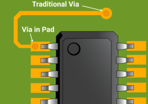
1.2 Basic Concept of Via-in-Pad Technology
At its core, Via-in-Pad Technology involves drilling a via hole (either plated through-hole or microvia) directly into the solder pad of a surface mount component. These vias are typically filled with conductive or non-conductive epoxy and then capped or plated over to provide a smooth, solderable surface. This process makes the pad usable for both electrical and mechanical connections while also serving as a conduit for inter-layer signal or power routing.
Although the concept sounds straightforward, its execution is complex. The filling, capping, and planarization processes require high precision and specialized materials to avoid issues like solder voiding, wicking, or component instability. This need for accuracy makes Via-in-Pad Technology particularly suitable for high-reliability applications such as aerospace, telecommunications, and medical devices.
1.3 Why This Technology Matters
The inclusion of vias directly within component pads can dramatically enhance PCB design capabilities. It allows for more efficient use of board real estate, supports the creation of smaller form factors, and improves electrical performance by reducing parasitic inductance and resistance. However, these benefits come with added complexity in manufacturing and cost.
The decision to use Via-in-Pad Technology should not be made lightly. It requires a careful assessment of the end-application, performance requirements, fabrication capabilities, and budgetary constraints. For some applications, the benefits will far outweigh the costs. For others, alternative via strategies might be more appropriate.
1.4 Scope of the Article
This article aims to provide an in-depth analysis of Via-in-Pad Technology in PCB Manufacturing, exploring its pros and cons from technical, financial, and practical perspectives. It will walk through the historical development, design principles, manufacturing techniques, application areas, and emerging trends. Special attention will be given to challenges such as reliability, thermal management, cost overhead, and supply chain considerations. The goal is to equip readers—engineers, designers, and decision-makers alike—with a comprehensive understanding that supports informed decision-making regarding this technology.
While the phrase Via-in-Pad Technology will be referenced in all major section headings, it will be used sparingly in the main body to maintain readability and reduce redundancy.
Via-in-Pad Technology
2. Historical Evolution of Via-in-Pad Technology in PCB Manufacturing
Understanding the historical backdrop of Via-in-Pad Technology in PCB Manufacturing provides valuable insight into why and how this technique has gained prominence. The journey from conventional through-hole technology to sophisticated via-in-pad configurations reflects broader shifts in electronics—toward miniaturization, performance optimization, and manufacturing precision.
2.1 Early Era: Through-Hole and Conventional Vias
Before surface mount technology (SMT) became widespread, through-hole technology dominated PCB design. Components had leads inserted through drilled holes and soldered on the opposite side. Vias, when present, were straightforward plated-through holes connecting different layers. They were never placed within component pads, since most components were mounted using mechanical leads.
This method was sufficient for simpler, low-density PCBs used in consumer electronics and industrial controls. However, as devices shrank and functionalities expanded, the limitations of through-hole methods—especially the need for larger boards—became increasingly evident.
2.2 Surface Mount Evolution and the Rise of Density Challenges
The introduction of SMT in the 1980s revolutionized PCB design. Components could now be mounted directly onto the surface of the PCB, enabling higher component densities and multi-layer designs. However, this evolution also brought a new set of challenges.
Designers started using smaller components with more pins and tighter spacing. As Ball Grid Array (BGA), Quad Flat No-lead (QFN), and Chip Scale Packages (CSPs) emerged, the traditional via placement outside the pad area became inefficient. Traces had to travel longer distances, leading to increased parasitic effects, signal degradation, and inefficient routing.
To counter this, via structures became more sophisticated. Microvias, blind and buried vias, and finally, vias directly in pads emerged as powerful solutions.
2.3 Early Adoption of Via-in-Pad Technology
The first significant use of Via-in-Pad Technology was seen in high-frequency RF and military/aerospace applications, where electrical performance outweighed cost considerations. These fields demanded minimal parasitic inductance, improved signal integrity, and compact layouts. Via-in-pad configurations offered a direct routing solution that helped achieve those goals.
In these early implementations, the manufacturing process was not fully optimized. Issues like solder wicking, planarity deviations, and voiding during reflow soldering were common. Nevertheless, the performance benefits were undeniable, prompting further investment in refining the technology.
2.4 Technological Advancements That Enabled Widespread Use
Over time, major improvements in materials science and process engineering made Via-in-Pad Technology in PCB Manufacturing more viable for broader applications:
-
Via Fill Materials: The development of conductive and non-conductive via-fill epoxies with controlled expansion coefficients helped reduce reliability issues like cracking and delamination.
-
Planarization Techniques: Advanced planarization methods such as CMP (Chemical Mechanical Planarization) and high-speed milling allowed for smoother pad surfaces that ensured reliable solder joints.
-
Laser Drilling and Microvia Fabrication: These enabled precise via creation in high-density designs, a cornerstone of modern HDI (High Density Interconnect) PCBs.
These innovations made via-in-pad more attractive to industries beyond aerospace and defense. Consumer electronics, medical devices, and automotive systems began incorporating the technique, especially as BGA pitch sizes decreased.
2.5 Standardization and Process Integration
By the early 2010s, Via-in-Pad Technology was no longer considered niche. PCB fabrication standards from IPC and JEDEC began to include guidelines for via-in-pad usage, and many fabrication houses built specialized capabilities for processing filled and capped vias. Integration into mainstream PCB design tools also contributed to faster adoption.
However, while the technology became more accessible, its successful implementation still required close collaboration between design engineers, fabricators, and assembly houses to avoid reliability pitfalls.
2.6 Current Status and Direction
Today, Via-in-Pad Technology in PCB Manufacturing is viewed as an advanced design technique that offers specific benefits in high-density, high-performance applications. It is no longer reserved exclusively for premium industries but is selectively used based on project needs and cost-benefit analysis.
Its evolution continues with innovations like stacked microvias, embedded passive components, and hybrid dielectric materials—all of which expand its applicability. Nonetheless, it remains a technique that must be approached thoughtfully, balancing advantages against fabrication complexity and long-term reliability.
3. Design Principles of Via-in-Pad Technology in PCB Manufacturing
Implementing Via-in-Pad Technology in PCB Manufacturing demands a fundamental rethinking of layout strategies, component placement, and signal routing. This section explores the design principles necessary to successfully integrate via-in-pad structures, addressing both functional and manufacturability considerations.
3.1 Understanding the Functional Role of Via-in-Pad
At its core, a via-in-pad connects internal or opposite PCB layers directly beneath a surface mount pad. This shortens signal paths, reduces parasitics, and enhances thermal conduction. In BGA packages, where traditional fan-out is limited due to pad pitch constraints, placing vias directly within pads becomes a design necessity rather than a luxury.
The functional benefits of these vias include:
-
Improved signal integrity, especially in high-speed digital or RF circuits
-
Effective thermal management, by dissipating heat through internal copper layers
-
Enhanced routing efficiency, especially in HDI (High Density Interconnect) boards
However, these benefits only manifest when the design adheres to precise standards and guidelines.
3.2 Key Layout Considerations for Via-in-Pad
Designers must account for the fact that vias located within pads require additional post-drilling processing steps, such as via filling and pad planarization. This affects both the pad stack-up and the PCB’s final surface finish.
Here are key layout practices:
-
Avoid large annular rings in via-in-pad designs to maintain pad integrity
-
Maintain controlled aspect ratios for microvias to ensure mechanical stability
-
Use filled and plated over vias to prevent solder wicking and air entrapment during assembly
-
Ensure symmetric via placement in critical power or differential signal nets to avoid skew and imbalance
CAD software often supports via-in-pad rules natively, allowing designers to define restrictions on via size, location, and fill type.
3.3 Choosing Between Conductive and Non-Conductive Via Fill
The choice of via fill material plays a significant role in both electrical performance and mechanical reliability. There are typically two types of fills used:
-
Conductive fill: Used when the via also functions as a thermal or electrical conduit. These are often employed under power pads or in high-frequency designs.
-
Non-conductive fill: Selected for general purposes where only mechanical support and solder mask integrity are needed.
Designers must weigh conductivity, thermal expansion, cost, and processing compatibility when making this choice.
3.4 Stack-up Design and Layer Planning with Via-in-Pad
Via-in-pad designs often appear in multilayer PCBs. Proper layer planning is crucial to avoid design bottlenecks or signal degradation. When using stacked microvias, designers must:
-
Avoid stacking more than two microvias on top of one another unless using reinforced substrates
-
Stagger vias where possible to distribute stress and maintain yield
-
Use internal ground or power planes for better heat sinking when thermal vias are used
-
Balance layer thicknesses to accommodate drilling and plating constraints
Effective use of simulation tools for impedance and thermal modeling can further validate design decisions.
3.5 Pad Design Guidelines to Support Via-in-Pad Structures
Unlike traditional SMT pads, pads in via-in-pad applications must withstand additional stress during assembly. Therefore:
-
Pads must be fully planarized to ensure smooth soldering
-
Solder mask defined (SMD) vs. non-solder mask defined (NSMD) pad decisions become critical, depending on mechanical loading
-
Use of underfill or edge bonding may be recommended for larger packages to manage thermomechanical stress
IPC standards such as IPC-4761 and IPC-7095 provide detailed guidance on pad design for via-in-pad scenarios.
3.6 Design for Manufacturability (DFM) with Via-in-Pad
Integrating via-in-pad requires closer collaboration between design engineers and PCB fabricators. Even when the electrical layout is sound, DFM rules must be respected to avoid production delays or yield issues.
Recommended practices include:
-
Sharing fabrication notes and layer stack-up diagrams with manufacturers early in the design phase
-
Specifying via fill requirements in the Gerber/ODB++ files
-
Adhering to the fabricator’s minimum via diameter and pad tolerances
-
Including test coupons to verify fill quality and adhesion during production runs
Many design rule checks (DRCs) related to via-in-pad can be automated within PCB CAD tools, though human oversight remains essential.
4. Manufacturing Processes Involved in Via-in-Pad Technology in PCB Manufacturing
The adoption of Via-in-Pad Technology in PCB Manufacturing introduces a series of specialized manufacturing steps that differ significantly from traditional via formation techniques. This section explores the sequence of processes required to implement via-in-pad structures, highlighting critical factors that affect quality, cost, and yield.
4.1 Drilling Techniques Specific to Via-in-Pad Applications
The via-in-pad manufacturing process begins with precise via drilling. Depending on the board’s complexity and the layer it connects, the drilling method can vary:
-
Mechanical drilling is commonly used for through-hole and buried vias. However, the tool wear and drill wander must be carefully managed due to the tight tolerances associated with via-in-pad.
-
Laser drilling is employed for microvias, particularly in HDI stack-ups, offering micron-level accuracy for small-diameter holes typically used in via-in-pad designs.
Key drilling considerations include:
-
Drill diameter control to match fill requirements
-
Drill depth accuracy in blind and stacked microvia configurations
-
Clean via wall preparation to support reliable plating adhesion
4.2 Desmearing and Cleaning of Drilled Vias
Post-drilling, the vias are subject to a desmear process to remove resin debris and prepare the via walls for metallization. This ensures electrical continuity and plating adhesion.
Typical methods include:
-
Plasma cleaning, especially effective in removing resin residues from high Tg laminates
-
Chemical desmear, utilizing permanganate or chromic acid solutions to etch away contaminants
-
Brushing and rinsing, used to mechanically and chemically treat via interiors
The cleaning process must be optimized for via-in-pad structures to prevent fill defects and plating irregularities.
4.3 Copper Deposition and Via Metallization
Next comes the electroless copper deposition stage, followed by electroplating to form the conductive via barrel. For via-in-pad designs, this metallization must be uniform and void-free, ensuring:
-
Electrical conductivity between layers
-
Sufficient mechanical strength
-
Reliable solder joint formation above the filled via
Special attention is required to:
-
Avoid overplating that might affect planarity
-
Ensure complete barrel coverage in stacked or blind via designs
-
Match plating thickness with via fill and surface finish plans
4.4 Via Filling: Conductive and Non-Conductive Fill Processes
The via fill process is critical in via-in-pad technology. It involves filling the drilled and plated vias with an epoxy-based material or a conductive paste. The choice of fill type affects thermal and electrical performance.
Non-conductive via fill:
-
Typically an epoxy compound
-
Used to isolate the via and prevent solder wicking
-
Provides mechanical support
Conductive via fill:
-
Filled with silver or copper-based pastes
-
Supports heat dissipation and electrical conduction
-
More expensive and complex to process
After filling, the material is cured in ovens under controlled conditions to ensure complete polymerization and structural integrity.
4.5 Surface Planarization of Filled Vias
Once filled, the surface of the via-in-pad must be planarized, ensuring that the pad is flat and smooth for component attachment. Uneven surfaces can lead to solder defects and misalignment during assembly.
Planarization methods include:
-
Mechanical grinding to level the pad
-
Chemical-mechanical polishing (CMP) for more advanced HDI boards
-
Planarization by plating in some cases, where a copper cap is plated over the via to level the surface
Planarization requires tight control to avoid removing too much material and compromising pad geometry.
4.6 Surface Finishing and Final Processing
The final manufacturing step involves applying a surface finish to the PCB to enhance solderability and protect copper traces. Common finishes used with via-in-pad include:
-
ENIG (Electroless Nickel Immersion Gold): Offers flatness and excellent wetting characteristics
-
OSP (Organic Solderability Preservative): Cost-effective, but less durable
-
ENEPIG (Electroless Nickel Electroless Palladium Immersion Gold): Suitable for wire bonding and more robust assemblies
The choice depends on the component type, budget, and performance requirements.
4.7 Inspection and Testing for Via-in-Pad Quality
Quality assurance in via-in-pad manufacturing is non-negotiable due to the risk of latent defects. Testing methods include:
-
X-ray inspection to detect internal voids and misalignment
-
Cross-sectioning for failure analysis and structure validation
-
Electrical testing for continuity and impedance
-
AOI (Automated Optical Inspection) to verify pad planarity and surface integrity
These inspections ensure that every via-in-pad functions correctly and meets IPC-6012 or other applicable industry standards.
5. Pros of Via-in-Pad Technology in PCB Manufacturing
The implementation of Via-in-Pad Technology in PCB Manufacturing has revolutionized how engineers and designers approach miniaturization, signal integrity, and thermal management in advanced circuit board design. This section examines the key advantages offered by this technology and explains why it is becoming increasingly common in high-density, high-performance electronic assemblies.
5.1 Space Optimization through Via-in-Pad Technology in PCB Manufacturing
One of the most compelling advantages of via-in-pad structures is the reduction in surface real estate consumption. In traditional PCB design, vias are typically located outside the component pads, requiring additional routing space.
Via-in-pad allows:
-
Direct placement of vias under component pads, maximizing space efficiency
-
Reduced PCB footprint, which is essential for compact devices such as smartphones, wearables, and medical implants
-
Better utilization of internal layers for routing, especially when multiple vias are stacked
This space-saving property enables engineers to integrate more functions into smaller boards without compromising performance or reliability.
5.2 Enhanced Electrical Performance from Via-in-Pad Technology in PCB Manufacturing
Signal integrity is a critical concern in modern electronics. The shortened interconnect lengths made possible by via-in-pad structures contribute directly to improved electrical behavior:
-
Lower inductance and resistance due to direct connections
-
Minimized parasitic effects, which benefits high-speed and high-frequency circuits
-
Improved impedance control, helping to preserve signal shape and timing in critical nets such as clocks or RF lines
These improvements are particularly advantageous in designs that implement DDR memory, high-speed serial interfaces, or analog-to-digital conversion.
5.3 Thermal Management Advantages of Via-in-Pad Technology in PCB Manufacturing
Another significant benefit of via-in-pad is superior thermal management. When implemented correctly, thermal vias within pads can conduct heat away from heat-generating components directly into internal copper planes or heat sinks.
Advantages include:
-
Efficient heat dissipation, which extends component life and improves performance
-
Enhanced thermal conductivity, especially when using conductive via fills
-
Reduced need for external heatsinks, leading to a more compact and cost-efficient system design
This is particularly important in LED lighting systems, power electronics, and CPU/GPU applications.
5.4 Improved Assembly and Soldering Outcomes in Via-in-Pad Technology in PCB Manufacturing
When designed and manufactured properly, via-in-pad also contributes to better SMT assembly results:
-
Flat and coplanar surfaces due to via filling and planarization eliminate voids in solder joints
-
Improved solder paste printing by avoiding solder migration into vias
-
Higher assembly yield rates due to more consistent soldering outcomes
This leads to increased production efficiency and reduced rework costs.
5.5 Compatibility with High-Density Interconnect (HDI) Boards via Via-in-Pad Technology in PCB Manufacturing
Via-in-pad technology integrates seamlessly with HDI PCB designs, which demand tightly packed components and fine line/space features. The combination of microvias, buried vias, and stacked vias in via-in-pad format enables:
-
Complex multilayer routing with fewer signal integrity issues
-
Layer reduction in some cases, simplifying the overall stack-up
-
Support for BGA packages with pitches under 0.5 mm, which would be impractical without via-in-pad implementation
This compatibility accelerates innovation in consumer electronics, aerospace, and networking infrastructure.
5.6 Higher Reliability in Rugged Environments with Via-in-Pad Technology in PCB Manufacturing
Finally, via-in-pad structures, when manufactured correctly, exhibit excellent mechanical stability:
-
Strong solder joints, due to even surfaces and proper metallization
-
Resilience to thermal cycling, especially when conductive fills are used
-
Lower failure rates under vibration or shock, thanks to shorter and more robust connections
These qualities make via-in-pad suitable for automotive electronics, avionics, and military systems where long-term reliability is critical.
6. Cons of Via-in-Pad Technology in PCB Manufacturing
While Via-in-Pad Technology in PCB Manufacturing brings significant advantages, it is equally important to consider the limitations and challenges associated with its implementation. This section will explore the key drawbacks, potential risks, and practical concerns that may arise during design, manufacturing, and assembly when using via-in-pad structures.
6.1 Increased Fabrication Costs Due to Via-in-Pad Technology in PCB Manufacturing
Perhaps the most notable downside of via-in-pad lies in its cost implications. Unlike traditional via drilling and plating, the via-in-pad process typically involves:
-
Laser drilling or micro-drilling, which is more precise and expensive
-
Via filling with conductive or non-conductive material, requiring additional time and resources
-
Surface planarization, such as copper plating or epoxy leveling, to ensure flatness
-
Additional inspection and reliability testing steps
These added processes increase both time and cost, making via-in-pad less attractive for low-budget or high-volume consumer electronics unless absolutely necessary.
6.2 Complexity in Manufacturing Process with Via-in-Pad Technology in PCB Manufacturing
The manufacturing workflow for via-in-pad is significantly more complex than standard through-hole or blind via production. Fabricators must carefully manage:
-
Fill material viscosity and conductivity, which can impact thermal or electrical performance
-
Void prevention during filling, especially for thermal pads
-
Precise planarization, to avoid dips that affect soldering
-
Stack-up design with controlled depth, especially in HDI boards
Even minor deviations in any step can result in poor yield rates, necessitating costly rework or scrapping of the board.
6.3 Risk of Solder Voiding in Via-in-Pad Technology in PCB Manufacturing
If vias are not properly filled and planarized, they may create voids or cavities in solder joints during reflow. These issues can result in:
-
Cold solder joints, reducing mechanical and electrical reliability
-
Solder wicking into unfilled vias, leading to insufficient solder volume on the pad
-
Open circuits or intermittent connectivity under thermal stress
These soldering issues are particularly problematic when dealing with BGA or LGA components, where visual inspection is not straightforward.
6.4 Limited Repairability in Via-in-Pad Technology in PCB Manufacturing
Another challenge lies in the difficulty of rework. Boards using via-in-pad are more sensitive to:
-
Delamination or pad lifting, especially when excessive heat is applied
-
Component removal and replacement, due to potential damage to filled vias
-
Thermal stress during soldering, which may weaken adjacent layers or cause cracks in the laminate
This limits the feasibility of field repairs or modifications and can raise total lifecycle costs for the product.
6.5 Longer Lead Time Associated with Via-in-Pad Technology in PCB Manufacturing
Because of the extra steps and precision required, lead times for via-in-pad boards are typically longer. This can delay product development schedules and increase time-to-market.
Factors contributing to the delay include:
-
More intricate CAM preparation and testing
-
Delays in via filling and curing
-
Stricter quality control and inspection standards
-
Possible iteration cycles due to low initial yields
Such lead time extensions may hinder rapid prototyping or agile hardware development environments.
6.6 Limited Vendor Capabilities for Via-in-Pad Technology in PCB Manufacturing
Not all PCB fabricators possess the technical capabilities or process maturity to execute via-in-pad reliably. The technology demands:
-
High-precision equipment for micro-via drilling and planarization
-
Controlled via fill chemistries and thermal treatment profiles
-
Robust quality management systems with IPC-6012 Class 3 capabilities or better
Limited access to qualified manufacturers may restrict options for sourcing, especially for startups or firms with smaller procurement volumes.
7. Design Guidelines for Via-in-Pad Technology in PCB Manufacturing
The effective use of Via-in-Pad Technology in PCB Manufacturing demands a thoughtful and detailed approach to design. To minimize the risks and leverage the benefits of this method, engineers must consider multiple layout, stack-up, and material factors. This section presents essential design guidelines that can help ensure manufacturability, reliability, and performance.
7.1 Pad Size and Via Diameter Considerations in Via-in-Pad Technology in PCB Manufacturing
To maintain integrity and solderability:
-
Pad sizes should be carefully selected based on the package type (e.g., BGA, QFN).
-
The via diameter must accommodate the pad while leaving sufficient annular ring.
-
Use smaller microvias (e.g., ≤0.15 mm) when space constraints demand tighter configurations.
Larger vias may require more complex filling and increase the risk of uneven surface height, which can complicate component placement.
7.2 Material Selection in Via-in-Pad Technology in PCB Manufacturing
Via-in-pad requires dielectric materials with specific thermal and electrical properties:
-
Low CTE (Coefficient of Thermal Expansion) laminates help minimize delamination under heat.
-
High-Tg materials resist deformation during soldering processes.
-
Compatible via-fill materials, such as conductive epoxy or copper, should match the thermal performance and chemical profile of the base laminate.
Choosing the right material stack-up improves reliability and simplifies processing.
7.3 Via Fill and Planarization in Via-in-Pad Technology in PCB Manufacturing
Proper filling of the via and surface planarization is critical to ensuring solder joint quality:
-
Fill vias with non-conductive epoxy for standard applications or copper for thermal and electrical continuity.
-
Vacuum-assisted via filling methods are preferred for uniform fill without voids.
-
Planarization (grinding or plating over) must maintain a flat surface within ±15 µm to avoid solder paste issues during SMT.
Incomplete filling or poor surface flatness often leads to solder bridging, tombstoning, or other defects.
7.4 Solder Mask Strategies in Via-in-Pad Technology in PCB Manufacturing
When using via-in-pad structures, solder mask application must be tightly controlled:
-
Avoid tenting or plugging on the same side of the pad where components are mounted.
-
Prefer via-in-pad with resin fill and cap plating, which does not require solder mask coverage on top.
-
Ensure solder mask clearance is sufficient to prevent mask slivers or bridging.
A well-executed solder mask design reduces the chance of solder migration and improves manufacturability.
7.5 Thermal Relief and Current Carrying Capacity in Via-in-Pad Technology in PCB Manufacturing
Via-in-pad designs must account for heat dissipation and current flow:
-
For high-power applications, use conductive via fill and thermal vias under power pads.
-
Employ multiple vias within large pads to distribute heat and current evenly.
-
Ensure adequate copper thickness in internal layers to handle expected power density.
Neglecting thermal design can result in hotspots, accelerated aging, or catastrophic failure.
7.6 PCB Stack-up Configuration in Via-in-Pad Technology in PCB Manufacturing
Via-in-pad has significant implications for PCB layer stack-up:
-
Avoid placing critical signal layers directly under via-in-pad pads to minimize signal distortion or thermal interference.
-
Use back-drilled stubs for signal integrity when vias pass through unused internal layers.
-
Ensure symmetrical construction to reduce board warpage during thermal cycling.
Optimized stack-up helps maintain impedance control, thermal balance, and mechanical strength.
7.7 DFM (Design for Manufacturability) Practices for Via-in-Pad Technology in PCB Manufacturing
Work closely with your PCB fabricator early in the design process:
-
Share complete IPC-compliant documentation (e.g., IPC-4761 for via types).
-
Confirm fill material compatibility, plating thickness tolerances, and process capabilities.
-
Consider design rule checks (DRC) that account for via-in-pad limitations.
Applying DFM principles reduces iteration cycles and increases yield in volume production.
8. Manufacturing Process Flow of Via-in-Pad Technology in PCB Manufacturing
Implementing Via-in-Pad Technology in PCB Manufacturing requires a precise and tightly controlled process flow. Each step must ensure structural integrity, electrical continuity, and surface flatness suitable for high-density component assembly. In this section, we examine the end-to-end manufacturing sequence and highlight critical process controls unique to via-in-pad designs.
8.1 Drilling and Via Formation in Via-in-Pad Technology in PCB Manufacturing
The process begins with precision drilling:
-
Laser drilling is often employed for microvias, especially in HDI (High-Density Interconnect) designs.
-
Mechanical drilling may be used for larger via diameters but must be tightly controlled to avoid pad damage or burr formation.
-
For stacked or staggered vias, depth control is essential to maintain layer-to-layer accuracy.
Post-drilling cleaning is necessary to remove debris and ensure good plating adhesion.
8.2 Via Plating and Copper Deposition in Via-in-Pad Technology in PCB Manufacturing
After the via holes are drilled:
-
Electroless copper deposition creates a conductive seed layer inside the via.
-
Electroplating builds up copper to the desired thickness, reinforcing electrical and structural strength.
-
In some cases, additional barrel plating may be performed to improve reliability, particularly for thermal or power vias.
The uniformity of plating is key, especially when vias are filled afterward.
8.3 Via Filling Techniques in Via-in-Pad Technology in PCB Manufacturing
This is one of the most defining steps in the via-in-pad process:
-
Conductive epoxy fill is common for signal vias, providing structural support and flattening the pad.
-
Copper via fill, often achieved through specialized plating chemistries, offers enhanced thermal and electrical performance.
-
Non-conductive epoxy fill may be selected when isolation is necessary between layers.
Filling must be complete and void-free to support soldering and avoid failures under thermal cycling.
8.4 Planarization and Surface Smoothing in Via-in-Pad Technology in PCB Manufacturing
After via filling:
-
Mechanical planarization (grinding or polishing) removes excess filler material.
-
This step ensures that the pad surface is flat and co-planar with adjacent pads, a prerequisite for accurate solder paste application.
-
Flatness is typically held within ±15 µm across the pad array.
Neglecting this stage can result in assembly defects such as tombstoning, poor solder joints, or uneven reflow.
8.5 Pad Plating and Surface Finish in Via-in-Pad Technology in PCB Manufacturing
The next critical process is plating the pad:
-
Electroless Nickel Immersion Gold (ENIG) is frequently used to provide a flat, solderable, and oxidation-resistant surface.
-
Electroless Nickel Electroless Palladium Immersion Gold (ENEPIG) may be used for more demanding applications.
-
OSP (Organic Solderability Preservative) is sometimes applied in cost-sensitive designs but may be unsuitable for fine-pitch BGA pads.
The surface finish must remain compatible with the chosen via fill and component assembly method.
8.6 Solder Mask Application in Via-in-Pad Technology in PCB Manufacturing
Solder mask application is performed post-planarization:
-
In via-in-pad designs, no solder mask is placed over the filled pad itself.
-
Instead, mask dams are applied between pads or around the perimeter of dense BGA arrays.
-
Laser-defined masks may be needed to maintain tight clearances on high-density layouts.
Solder mask registration is critical to prevent sliver defects or bridging.
8.7 Assembly and Reflow in Via-in-Pad Technology in PCB Manufacturing
Assembly processes must accommodate the unique via-in-pad structure:
-
Solder paste printing benefits from flat, void-free pad surfaces created through via filling and planarization.
-
During component placement, accurate Z-height and vacuum pickup are essential for fine-pitch components.
-
Reflow soldering profiles should be optimized to avoid excessive thermal stress on filled vias.
Smooth solder joint formation ensures performance in high-frequency and high-reliability environments.
8.8 Inspection and Quality Control in Via-in-Pad Technology in PCB Manufacturing
Rigorous inspection is mandatory throughout the process:
-
X-ray inspection verifies via fill quality and solder joint formation.
-
AOI (Automated Optical Inspection) checks for mask registration, pad geometry, and solder paste accuracy.
-
Cross-section analysis is used in sampling to inspect internal via quality and ensure plating integrity.
Advanced quality control is especially important in aerospace, medical, or automotive PCBs where via failure is unacceptable.
9. Reliability Considerations of Via-in-Pad Technology in PCB Manufacturing
Reliability is one of the most critical aspects when adopting Via-in-Pad Technology in PCB Manufacturing, especially for applications in aerospace, medical electronics, high-speed computing, and telecommunications. In this section, we explore the key factors influencing the reliability of this technology, as well as common failure modes, testing protocols, and long-term performance characteristics.
9.1 Mechanical Reliability in Via-in-Pad Technology in PCB Manufacturing
Via-in-pad designs are sensitive to mechanical stresses:
-
Thermo-mechanical stress caused by CTE (Coefficient of Thermal Expansion) mismatch between different materials may lead to delamination or cracking around the vias.
-
Warpage and bowing of the board, especially in large PCBs or multilayer HDI boards, can stress the filled vias if not properly managed.
-
For portable devices, drop and vibration testing is often required to validate the mechanical robustness of the via structure.
Proper material selection and structural modeling during design can improve performance under physical stress.
9.2 Thermal Cycling and Fatigue in Via-in-Pad Technology in PCB Manufacturing
Thermal fatigue is a leading cause of failure in PCBs using via-in-pad technology:
-
Repeated temperature cycling (e.g., in automotive electronics) can cause copper fatigue inside filled vias, leading to cracks and open circuits.
-
Voids in via fill material exacerbate thermal stress concentration.
-
Thermal cycling tests such as IPC-TM-650 2.6.7.2 can reveal vulnerabilities in via design and construction.
Using filled copper vias and applying stress-relief geometries can extend the board’s service life.
9.3 Electrical Integrity in Via-in-Pad Technology in PCB Manufacturing
High-speed and high-frequency applications demand uncompromised electrical integrity:
-
Poor via fill or plating inconsistencies can result in impedance discontinuities, which cause signal reflection and attenuation.
-
Parasitic inductance or capacitance from poorly terminated vias can impact signal timing and EMI performance.
-
Electromigration under high current density may also impact long-term via reliability.
Advanced simulation and impedance control in the layout stage are necessary for optimizing signal performance.
9.4 Moisture Sensitivity and Outgassing in Via-in-Pad Technology in PCB Manufacturing
Moisture trapped in vias or filler material poses a risk:
-
During reflow soldering, moisture-induced outgassing can result in solder voids or pad delamination.
-
Some via-fill epoxies are more hydrophilic than others, making material selection critical for humid environments.
-
Boards should be baked before assembly to mitigate moisture absorption and reduce outgassing risks.
Conformal coatings can be added for applications requiring environmental sealing.
9.5 Chemical Resistance and Environmental Durability in Via-in-Pad Technology in PCB Manufacturing
Via-in-pad reliability can degrade when exposed to harsh environments:
-
Chemicals in flux, cleaning agents, or field exposure can erode filler material or plating layers if not properly selected.
-
ENIG and ENEPIG finishes offer good corrosion resistance but must be well controlled during deposition.
-
In marine, industrial, or outdoor environments, salt spray and pollution tests are recommended to verify resistance.
Material compatibility must be carefully validated for mission-critical PCBs.
9.6 Testing Methods for Via-in-Pad Technology in PCB Manufacturing
To assure quality, the following tests are commonly performed:
-
Thermal shock testing to simulate rapid temperature changes.
-
Shear and pull tests to check the adhesion and strength of filled pads.
-
Micro-sectioning and SEM imaging to examine internal via integrity and detect micro-cracks or voids.
Reliability test data helps in qualification for IPC Class 2 or Class 3 applications.
9.7 Lessons from Field Failures in Via-in-Pad Technology in PCB Manufacturing
Real-world use cases have highlighted several recurring failure mechanisms:
-
Improper planarization can lead to solder joint failure under thermal cycling.
-
Incomplete via fill or poor epoxy curing can introduce mechanical weaknesses.
-
Lack of impedance control in high-speed designs has led to signal degradation and field returns.
10. Cost Implications of Via-in-Pad Technology in PCB Manufacturing
Adopting Via-in-Pad Technology in PCB Manufacturing brings several cost considerations that need careful evaluation, especially for manufacturers looking to balance performance and production costs. This section explores the cost factors involved in designing, fabricating, and assembling PCBs with via-in-pad technology, as well as ways to manage costs without compromising quality.
10.1 Initial Design and Engineering Costs in Via-in-Pad Technology in PCB Manufacturing
The initial design phase for PCBs using via-in-pad technology is typically more expensive than traditional designs:
-
Design complexity increases due to the need to account for via filling, plating, and pad optimization.
-
Simulation tools and advanced PCB design software capable of modeling via-in-pad configurations and their electrical and mechanical behavior are often required.
-
Materials selection for both via fill and PCB layers adds to the cost, as specialized materials (e.g., conductive epoxy) may be needed to meet performance specifications.
Although these costs may be higher initially, the payoff in performance and reliability can justify the expense in high-performance applications.
10.2 Increased Manufacturing Costs in Via-in-Pad Technology in PCB Manufacturing
The manufacturing process for via-in-pad technology introduces additional costs at several stages:
-
Drilling and via formation: Laser drilling and precision mechanical drilling are necessary to ensure clean vias for filling, and these processes often require more specialized equipment and higher maintenance.
-
Via filling: The need for specialized via fill material (e.g., conductive or non-conductive epoxy) and techniques (e.g., pressure curing, controlled heating) increases material and labor costs.
-
Planarization and surface finishing: The process of ensuring a flat, even surface for the pads often requires additional mechanical or chemical treatments, which adds time and resources to the process.
-
Additional plating and solder mask considerations also contribute to higher costs.
Each of these stages must be optimized to avoid delays and additional expenses while maintaining quality standards.
10.3 Assembly Costs in Via-in-Pad Technology in PCB Manufacturing
The assembly process for PCBs with via-in-pad technology can be more expensive compared to traditional designs:
-
Solder paste printing requires precision to ensure that the filled vias do not interfere with paste placement.
-
Component placement on via-in-pad designs demands more advanced pick-and-place machines, as they must accommodate varying pad heights and align with fine-pitch components.
-
The reflow soldering process must be carefully controlled to avoid damaging via fills or causing solder defects.
-
Inspection and testing: High levels of inspection (e.g., X-ray inspection, optical inspection) are often necessary to ensure proper via fill and solder joint integrity. These tests add significant cost, especially for higher-end PCBs used in demanding applications.
While these added costs may increase overall assembly expenses, they are a necessary investment in ensuring the PCB’s reliability and performance.
10.4 Yield Loss and Scrap in Via-in-Pad Technology in PCB Manufacturing
Yield loss and scrap rates are often higher with via-in-pad technology, which can further drive up costs:
-
Manufacturing defects: Poor via filling or planarization issues can lead to defective boards that must be scrapped or reworked.
-
Overfill or underfill of vias can result in weak mechanical bonds or electrical failures, making the board unusable.
-
Thermal stress or mechanical failure during handling or testing may lead to rework or rejection.
While careful process control can reduce these defects, the higher complexity associated with via-in-pad technology typically results in a higher scrap rate, which impacts cost efficiency.
10.5 Long-Term Cost Savings and Return on Investment (ROI) in Via-in-Pad Technology in PCB Manufacturing
Despite the higher initial and manufacturing costs, via-in-pad technology can offer long-term savings in certain applications:
-
Space-saving design: The ability to integrate more components into a smaller PCB footprint allows for the creation of compact and lightweight devices, which is particularly advantageous in consumer electronics, automotive, and medical devices.
-
Enhanced reliability: The durability and performance of via-in-pad PCBs reduce the risk of product failure, leading to lower warranty claims and longer product lifespans.
-
Higher throughput: In high-volume production environments, via-in-pad technology can lead to more efficient PCB assembly, reducing overall labor costs and increasing output rates.
-
Improved performance: By facilitating the use of high-speed components and reducing the risk of signal integrity issues, via-in-pad technology can offer better electrical performance, which may be crucial for products requiring high-frequency operation.
In the long run, these advantages can result in a positive ROI, especially for mission-critical applications.
10.6 Cost Reduction Strategies in Via-in-Pad Technology in PCB Manufacturing
Several strategies can be implemented to help reduce costs associated with via-in-pad technology:
-
Design optimization: Early-stage design modifications to minimize the number of vias or use fewer layers can reduce the complexity and cost of manufacturing.
-
Material cost management: Sourcing cost-effective materials for via filling and plating without compromising quality can help control material expenses.
-
Automation and process improvements: Implementing automated systems for drilling, filling, planarization, and testing can improve efficiency, reduce labor costs, and enhance overall throughput.
-
Supplier collaboration: Partnering with reliable suppliers to source high-quality, cost-effective via fill materials, coatings, and plating solutions can reduce material costs.
-
Testing and inspection improvements: Streamlining the testing and inspection processes, using advanced in-line testing methods, can reduce the time and costs associated with final product verification.
By focusing on these cost-saving strategies, manufacturers can mitigate the financial impact of via-in-pad technology while maintaining high-quality standards.
11. Future Trends in Via-in-Pad Technology in PCB Manufacturing
As the electronics industry continues to evolve, Via-in-Pad Technology in PCB Manufacturing is likely to see significant advancements. With growing demand for miniaturized, high-performance, and reliable electronic products, manufacturers are continuously seeking ways to improve the capabilities of via-in-pad technology. This section explores some of the potential future trends in via-in-pad technology, addressing innovations, emerging materials, and evolving manufacturing processes.
11.1 Advances in Via Filling Materials in Via-in-Pad Technology
The development of new via filling materials is a major area of focus for improving via-in-pad technology:
-
Nanomaterials: Nanotechnology holds the potential to create stronger, more reliable, and thermally stable via-fill materials. Nanocomposites could enhance the mechanical properties and reduce the chances of delamination or cracking.
-
Conductive polymers: Research into conductive polymer-based via-fill materials may lead to more flexible solutions with better electrical performance and lower costs than traditional metal-based fillers.
-
Thermally conductive materials: As demand for heat dissipation increases, the development of via fills with enhanced thermal conductivity is likely to become a key trend, especially in high-power applications such as automotive or industrial systems.
-
Self-healing materials: Innovations in self-healing polymers or epoxy systems could offer self-repairing capabilities for vias, improving long-term reliability and performance.
These advancements could reduce manufacturing defects, improve overall yield, and enhance the performance of via-in-pad designs.
11.2 Integration of Artificial Intelligence and Machine Learning in Via-in-Pad Technology
Artificial intelligence (AI) and machine learning (ML) are increasingly being adopted in PCB design and manufacturing, and via-in-pad technology is no exception:
-
Design optimization: AI-driven algorithms can assist in optimizing via-in-pad placements, material selection, and even via-filling processes by learning from large datasets and previous designs.
-
Predictive maintenance: Machine learning models can be used to predict when equipment is likely to fail, allowing manufacturers to proactively maintain machines and avoid disruptions in the production process.
-
Automated inspection: AI-powered inspection systems can enhance the quality control process, identifying potential defects in via fill, planarization, or soldering that might be missed by traditional methods.
Incorporating AI and ML into via-in-pad manufacturing will likely lead to smarter, more efficient production processes with fewer defects and improved cost-effectiveness.
11.3 Miniaturization and High-Density Interconnects (HDI)
Miniaturization continues to drive the evolution of via-in-pad technology, particularly in the field of high-density interconnect (HDI) boards:
-
Smaller components: As electronic devices shrink in size, the need for high-density PCBs increases. Via-in-pad technology enables designers to integrate more components into smaller areas, facilitating compact and high-performance devices.
-
Microvias: The use of microvias in conjunction with via-in-pad technology will become more prevalent, allowing for the integration of ultra-small vias and better signal integrity in high-speed applications.
-
Multilayer and 3D PCBs: The trend toward 3D PCB stacking and multilayer designs will further push the adoption of via-in-pad technology, as these structures require precise via placement and filling techniques to ensure electrical performance and reliability.
This trend will continue to drive the development of advanced via-in-pad technologies capable of meeting the stringent requirements of high-density and miniaturized electronics.
11.4 Environmentally Friendly and Sustainable Solutions
Sustainability is becoming increasingly important in the electronics industry, and via-in-pad technology will need to adapt to meet environmental demands:
-
Eco-friendly via-fill materials: There is growing interest in developing environmentally friendly alternatives to traditional via-fill materials. These could include bio-based resins, non-toxic fillers, or recyclable materials.
-
Energy-efficient manufacturing: As PCB manufacturers strive to reduce their carbon footprint, there will be an emphasis on energy-efficient production processes, such as more efficient curing techniques or greener soldering methods that do not rely on harmful chemicals.
-
Waste reduction: Advanced manufacturing techniques, such as additive manufacturing (3D printing), may help reduce waste in the PCB production process by enabling more precise material deposition and reducing excess material use.
By focusing on sustainability, the PCB industry can help reduce its environmental impact while maintaining high-quality production standards.
11.5 Advanced Manufacturing Technologies for Via-in-Pad Technology
The future of via-in-pad technology will also be shaped by innovations in manufacturing equipment and techniques:
-
Laser direct structuring (LDS): LDS technology, which allows for direct structuring of PCBs without the need for traditional photoresist and etching processes, could enhance via-in-pad fabrication by improving precision and reducing process time.
-
3D printing of PCBs: The integration of additive manufacturing for PCB production could enable the creation of complex via structures and pad designs that are difficult or impossible to achieve with traditional subtractive methods. This could be especially useful in prototyping or small-batch production of highly customized boards.
-
Roll-to-roll processing: This technique, often used in flexible electronics, may be adapted for high-volume production of via-in-pad technology, providing faster, lower-cost manufacturing for flexible PCBs.
These emerging technologies will likely revolutionize the production of via-in-pad designs, offering more cost-effective, precise, and scalable solutions for the electronics industry.
11.6 Enhanced Electrical Performance for High-Speed and High-Frequency Applications
As the demand for high-speed and high-frequency applications continues to grow, via-in-pad technology will play an essential role in enabling optimal electrical performance:
-
Signal integrity: To meet the requirements of 5G, high-speed networking, and high-frequency communications, via-in-pad designs will need to be carefully engineered to minimize impedance discontinuities, crosstalk, and signal loss.
-
Impedance-controlled designs: Future advances in via-in-pad technology will likely focus on achieving better impedance control by utilizing more precise via-filling techniques and novel materials that reduce the parasitic effects of vias.
-
Lower insertion loss and crosstalk: As bandwidth demands increase, future via-in-pad designs will need to ensure minimal signal distortion by improving the electrical properties of vias and pad designs.
In this regard, via-in-pad technology will continue to evolve to meet the growing demands of high-performance computing, telecommunications, and other high-speed applications.
11.7 Collaboration Between Industry and Academia for Innovation
To further advance via-in-pad technology, collaboration between industry leaders and academic researchers will be critical:
-
Research and development (R&D) efforts focusing on new materials, designs, and processes will continue to push the boundaries of what is possible with via-in-pad technology.
-
Academic partnerships with industry can help drive innovation by offering insights into new manufacturing techniques, material science advancements, and performance modeling.
-
Industry-sponsored research initiatives may also focus on solving specific challenges such as reducing cost, improving yield, and enhancing reliability in high-performance applications.
Collaborative efforts between industry and academia will likely accelerate the development of next-generation via-in-pad technologies.
12. Conclusion: The Balanced View of Via-in-Pad Technology in PCB Manufacturing
Via-in-pad technology, while offering substantial advantages in terms of design flexibility, miniaturization, and enhanced performance, also presents significant challenges that must be carefully managed to ensure reliable PCB manufacturing. As with any advanced technology, understanding both its benefits and limitations is crucial for manufacturers, designers, and engineers who seek to leverage it in their PCB designs.
12.1 Recap of the Pros of Via-in-Pad Technology
Throughout this article, we’ve discussed several key benefits that via-in-pad technology brings to PCB manufacturing:
-
Design flexibility and miniaturization: Via-in-pad technology allows for compact designs and the integration of more components in smaller spaces. This is particularly beneficial in applications that demand high performance in limited space, such as mobile devices, wearables, and automotive electronics.
-
Improved signal integrity: In high-frequency and high-speed applications, via-in-pad technology can be used to reduce signal distortion, ensuring better performance in demanding environments like 5G communication systems and advanced computing hardware.
-
Simplified PCB design: Via-in-pad offers designers the ability to streamline PCB layouts by allowing vias to be placed directly under pads, which eliminates the need for complex routing around traditional vias.
12.2 Recap of the Cons and Challenges of Via-in-Pad Technology
While via-in-pad technology provides numerous benefits, it also comes with its own set of challenges:
-
Manufacturing complexity: The integration of vias within pads can create challenges during manufacturing, particularly with via filling, planarization, and soldering. These processes require precise control to avoid defects like voids or poor adhesion.
-
Cost considerations: The use of via-in-pad technology often leads to higher production costs due to the need for specialized materials, equipment, and process adjustments. These additional costs may not be justified in all applications.
-
Reliability concerns: The potential for thermal expansion mismatches, mechanical stress, and delamination in via-in-pad designs poses a risk to long-term reliability, especially in harsh operating environments.
12.3 Future Outlook for Via-in-Pad Technology
As technology continues to advance, the future of via-in-pad technology looks promising, but it will need to adapt to meet the increasing demands of the industry:
-
Enhanced materials: Ongoing research into advanced materials for via-filling and pad design is expected to result in more reliable, cost-effective, and environmentally friendly solutions.
-
Improved manufacturing techniques: As PCB manufacturing technology progresses, innovations in automation, 3D printing, and precision machining will likely help overcome many of the existing challenges related to via-in-pad production.
-
Increased adoption: As the need for high-density and high-performance electronics grows, via-in-pad technology is expected to become more widely adopted across a variety of industries, from consumer electronics to automotive and aerospace.
12.4 The Balance Between Pros and Cons
Ultimately, whether via-in-pad technology is the right choice for a particular PCB design depends on the specific requirements and constraints of the project. While the benefits in terms of design flexibility, compactness, and signal integrity are compelling, the associated manufacturing challenges and higher costs may make it less suitable for certain applications. A balanced approach—carefully considering the advantages and disadvantages—is essential for making informed design and manufacturing decisions.
In conclusion, via-in-pad technology is a powerful tool in the PCB designer’s toolkit, offering solutions to meet the growing demands of modern electronics. By carefully managing the challenges, manufacturers can take full advantage of this innovative technology, paving the way for more efficient, high-performance electronic devices in the future.

- long board pcb
- Flexible PCBs
- Special PCB
- Express Printed Circuit Board
- Pcb Prototype
- LED PCB
- PCB
- Printed Circuit Board
- Pcb meaning
- Pcb manufacturer
- Rigid pcb board
- Rigid Flex PCB
 Quote
Quote
 E-mail