Introduction to Impedance Test
1.1 Understanding Impedance in PCBs
Printed circuit boards (PCBs) serve as the backbone of modern electronics, enabling the seamless transmission of electrical signals between components. With the increasing demand for high-speed and high-frequency applications, controlling impedance in PCB designs has become crucial. The Impedance Test is a critical quality control step that ensures PCBs meet the necessary electrical performance requirements.
In simple terms, impedance is the measure of opposition a circuit presents to the flow of alternating current (AC). Unlike resistance, which applies to direct current (DC) circuits, impedance considers both resistive and reactive elements, including capacitance and inductance. Impedance control is essential in high-frequency applications where signal integrity, transmission speed, and electromagnetic compatibility (EMC) are major concerns.
As electronic devices become increasingly sophisticated, the need for reliable and high-performance printed circuit boards (PCBs) grows exponentially. One of the most critical factors in ensuring a PCB’s optimal functionality is impedance control, which directly affects signal integrity and performance. The Impedance Test is a crucial quality assurance step that helps verify whether the PCB meets the required electrical characteristics.
Impedance refers to the total opposition a circuit element presents to the flow of alternating current (AC). It comprises resistance, capacitance, and inductance components, making it a key consideration for PCB manufacturers designing high-speed digital and radio-frequency (RF) circuits. Unlike low-frequency circuits, where resistance is the primary concern, high-frequency circuits require precise impedance matching to minimize signal loss, reflections, and interference.
In modern electronic applications such as 5G telecommunications, automotive radar systems, and high-speed computing, impedance control ensures seamless transmission of data. Without proper impedance matching, electronic signals can become distorted, leading to malfunctions, increased power loss, and decreased efficiency.
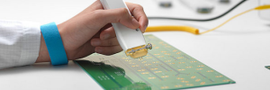
Impedance Test
The Importance of Impedance Control in PCB Design
The Impedance Test is not just an additional step in PCB production; it is an integral aspect of ensuring circuit reliability. PCB designers must carefully calculate impedance values during the design phase to prevent signal degradation, crosstalk, and unwanted reflections. The necessity of controlled impedance is most apparent in applications involving:
-
High-speed data transmission (e.g., HDMI, USB, PCIe, Ethernet)
-
RF and microwave communication
-
Medical electronics requiring precision signal processing
-
Aerospace and defense systems where reliability is paramount
By implementing impedance control early in the design process, engineers can create circuits that perform consistently under various operating conditions. However, merely designing for impedance control is not sufficient. The actual manufacturing process must also align with design expectations, making Impedance Testing a crucial post-production validation step.
1.2 Importance of Impedance Test in PCB Manufacturing
The Impedance Test is not just a verification step; it is a fundamental process that determines the reliability and performance of PCBs. Without proper impedance control, electronic circuits can suffer from signal loss, distortion, and interference, ultimately leading to device malfunctions.
Key reasons why impedance testing is crucial include:
-
Signal Integrity: Ensures that high-frequency signals propagate without significant degradation.
-
EMI Reduction: Helps minimize electromagnetic interference (EMI) in circuits.
-
Compliance with Industry Standards: Many industries, including telecommunications, automotive, and aerospace, have strict impedance control requirements.
-
Reliability of High-Speed PCBs: In applications like 5G networks, IoT devices, and RF communication, maintaining controlled impedance is non-negotiable.
1.3 How Impedance Test is Conducted
The Impedance Test typically involves measuring the characteristic impedance of PCB traces using advanced testing equipment. Manufacturers use time-domain reflectometry (TDR) and vector network analyzers (VNA) to assess impedance values and compare them against predefined specifications. The test is performed at different points along signal traces to ensure uniform impedance throughout the PCB.
2. Impedance Test Methods and Equipment
2.1 Time-Domain Reflectometry (TDR)
One of the most common methods for impedance testing is Time-Domain Reflectometry (TDR). This technique involves sending a fast-rising pulse through a PCB trace and measuring the reflections caused by impedance mismatches. If the impedance deviates from the target value, part of the signal reflects back to the source, allowing engineers to pinpoint issues in the transmission line.
Advantages of TDR in Impedance Testing
-
Provides real-time analysis of impedance variations along the trace.
-
Detects open circuits, short circuits, and discontinuities in signal traces.
-
Highly accurate for high-frequency PCB designs.
Limitations of TDR Testing
-
Requires high-end, expensive equipment.
-
May not be suitable for very fine-pitch PCB designs with complex routing.
2.2 Vector Network Analyzer (VNA) Testing
Another advanced method is using a Vector Network Analyzer (VNA). Unlike TDR, which works in the time domain, a VNA operates in the frequency domain, measuring S-parameters to analyze impedance characteristics.
Advantages of VNA Testing
-
More precise for analyzing frequency-dependent impedance variations.
-
Useful for RF and microwave PCB applications.
-
Allows for multiple port measurements and complex impedance modeling.
Challenges of VNA Testing
-
Requires a deep understanding of signal processing and S-parameter interpretation.
-
Expensive and may not be necessary for simpler PCB designs.
2.3 Other Impedance Testing Techniques
Other testing methods include:
-
Resonance-based impedance measurement (used in RF applications).
-
LCR meters for low-frequency impedance testing.
-
On-board test structures designed into the PCB layout for in-situ testing.
3. Factors Affecting PCB Impedance and Testing Accuracy
3.1 PCB Material Selection
The dielectric constant (Dk) of PCB materials significantly impacts impedance. Common materials include:
-
FR4: Standard material with moderate Dk (≈4.2).
-
Rogers laminates: High-performance materials for RF applications with stable Dk.
-
PTFE-based materials: Used for ultra-high-frequency PCBs.
3.2 Trace Geometry and Layout
The width, thickness, and spacing of PCB traces affect impedance. Designers must follow strict impedance matching guidelines to ensure signal integrity.
3.3 Manufacturing Variations
Slight inconsistencies in etching, plating, or lamination can alter impedance values. Manufacturers must maintain tight tolerances in production.
4. Industry Standards and Requirements for Impedance Test
Various industry standards govern impedance control in PCBs, including:
-
IPC-2141: Provides guidelines for impedance calculation.
-
ISO 9001: Ensures manufacturing quality control.
-
IEEE 802.3: Defines Ethernet signal transmission requirements.
Compliance with these standards ensures that PCBs function reliably in different electronic applications.
5. Challenges and Solutions in Conducting Impedance Test
5.1 Common Challenges
-
Material Variability: Differences in dielectric properties can lead to inconsistent impedance values.
-
Complexity in High-Layer PCBs: Multilayer PCBs require precise impedance control for multiple signal layers.
-
Equipment Cost: Advanced impedance testing equipment can be expensive.
5.2 Solutions
-
Use automated impedance control software during PCB design.
-
Implement rigorous material selection and supplier evaluation.
-
Optimize manufacturing processes to reduce variability.
6. Future Trends in PCB Impedance Testing
6.1 AI and Machine Learning for Impedance Analysis
Artificial Intelligence (AI) and machine learning algorithms are being integrated into impedance testing systems to improve accuracy and predictive analysis.
6.2 Advanced Materials for Stable Impedance Control
New composite materials with ultra-low Dk variations are being developed for high-speed PCBs.
6.3 Miniaturization and Higher Frequencies
As PCBs become smaller and operate at higher frequencies (e.g., 5G, IoT), impedance control will become even more critical.
7. Conclusion: The Evolving Role of Impedance Test in PCB Manufacturing
Recap of the Role of Impedance Test in PCB Manufacturing
The Impedance Test is a cornerstone of modern PCB manufacturing, playing a vital role in ensuring signal integrity, reducing electromagnetic interference (EMI), and maintaining circuit performance across various applications. Whether a PCB is used in high-speed data transmission, RF communication, or automotive safety systems, impedance control remains a critical factor in overall device functionality.
Throughout this discussion, we have explored:
-
The importance of impedance control in PCB design.
-
The various testing methods, including TDR and VNA, that enable precise impedance measurements.
-
The challenges and solutions associated with maintaining impedance consistency.
-
The evolving industry standards and best practices that help manufacturers achieve high-quality PCBs.
As electronic devices become faster and more complex, Impedance Testing will only grow in significance. New technologies, advanced materials, and automated testing methodologies will be required to meet the increasing demands of next-generation circuit boards.
Emerging Trends in Impedance Testing and PCB Manufacturing
Looking ahead, several key trends are shaping the future of Impedance Testing in PCB manufacturing:
-
AI-Powered Impedance Analysis: Artificial intelligence and machine learning are being integrated into impedance analysis tools to predict signal integrity issues and optimize PCB layouts automatically. AI-driven simulations can identify impedance mismatches before the manufacturing stage, reducing design iterations and production costs.
-
Advanced Materials for Better Impedance Control: Manufacturers are investing in next-generation materials with highly stable dielectric properties. Low-loss, high-frequency laminates are increasingly being used to maintain consistent impedance across various temperature and environmental conditions.
-
Miniaturization and High-Density Interconnects (HDI): With the rise of compact electronic devices, high-density interconnect (HDI) PCBs require even more stringent impedance control. Innovations in PCB stack-up configurations and microvia technology are making impedance testing even more critical in ensuring reliable signal transmission.
-
Integration of 5G and High-Frequency PCB Design: The rapid deployment of 5G networks and millimeter-wave (mmWave) technology is pushing PCB manufacturers to refine impedance control techniques. Impedance mismatches in these high-frequency circuits can cause severe performance degradation, making Impedance Testing an essential validation process.
-
Automation and Real-Time Monitoring of Impedance: The future of impedance testing includes real-time monitoring during PCB manufacturing. Automated inline impedance measurement tools are being developed to identify deviations instantly, reducing the need for manual rework and improving overall production efficiency.
7.1 Summary of Key Points
The Impedance Test plays a crucial role in ensuring the functionality and reliability of high-speed PCBs. With the increasing complexity of electronic devices, manufacturers must adopt advanced testing methods to maintain strict impedance control.
7.2 Looking Ahead
Future advancements in automated impedance testing, AI-driven analysis, and next-generation materials will further enhance the precision and efficiency of PCB manufacturing. Companies investing in these technologies will gain a competitive advantage in the rapidly evolving electronics industry.
7.3 Final Thoughts
Maintaining controlled impedance through rigorous testing is not just a technical necessity—it is a fundamental requirement for the future of high-performance electronic systems. As PCB technology advances, so too will the methods for ensuring optimal impedance characteristics.

- long board pcb
- Flexible PCBs
- Special PCB
- Express Printed Circuit Board
- Pcb Prototype
- LED PCB
- PCB
- Printed Circuit Board
- Pcb meaning
- Pcb manufacturer
- Rigid pcb board
- Rigid Flex PCB
 Quote
Quote
 E-mail