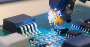
Introduction to Component Hole in PCB
Component holes are an essential feature in PCB (Printed Circuit Board) design, facilitating the secure mounting and soldering of electronic components. They serve as mechanical and electrical connections between different PCB layers, allowing current flow through plated through-holes (PTH) or securing components with non-plated through-holes (NPTH). The precision and integrity of component holes significantly impact PCB performance, reliability, and manufacturability.
This article provides a comprehensive overview of component hole technology, its classification, manufacturing considerations, common challenges, and best practices in PCB production.
In the world of printed circuit boards (PCBs), component holes play a fundamental role in determining the mechanical and electrical integrity of the board. These holes serve as mounting points for electronic components, enabling them to be securely attached to the board while also facilitating electrical connections between different layers in multilayer PCBs. Whether for through-hole technology (THT) components, vias, or mechanical mounting, the design and manufacturing of component holes require careful planning and precision engineering to ensure optimal performance.
This introduction provides a detailed look at the significance of component holes, their impact on PCB design, and the best practices to ensure reliability and manufacturability in modern electronic circuits.
Component holes
The Role of Component Hole in PCB Design
Component holes in PCBs are primarily classified into plated through-holes (PTH), non-plated through-holes (NPTH), and vias, each serving different purposes in circuit board assembly and functionality.
-
Plated Through-Hole (PTH): These holes are electroplated with a thin copper layer, allowing electrical connectivity between different PCB layers. They are widely used for THT components, which require leads to pass through the board for soldering.
-
Non-Plated Through-Hole (NPTH): These holes are primarily used for mechanical purposes, such as securing screws, connectors, or mounting points. They do not have a conductive coating and do not participate in electrical pathways.
-
Vias: These are small holes that connect different PCB layers electrically. Unlike PTHs, vias do not accommodate component leads but serve as electrical pathways for signal transmission.
The selection of component hole types and their precise placement significantly influence PCB performance, particularly in terms of mechanical stability, electrical reliability, and heat dissipation.
Evolution of Component Hole Technology
With advancements in PCB technology, component hole fabrication has evolved significantly to meet the increasing demands of modern electronics.
1. Early PCB Manufacturing Techniques
In early PCB production, component holes were primarily drilled mechanically using carbide-tipped drill bits. These processes required manual alignment and had limited precision, leading to challenges such as hole misalignment and inconsistencies in hole wall quality.
2. Introduction of Plated Through-Holes (PTHs)
As electronic circuits became more complex, the need for multilayer connectivity led to the adoption of plated through-hole (PTH) technology. This advancement allowed PCB designers to create more compact and efficient circuits by enabling electrical connections between multiple layers.
3. High-Density Interconnect (HDI) and Microvia Technology
The rise of HDI PCBs introduced microvias—tiny component holes created using laser drilling. These microvias allow for high-density interconnections, reducing the size and weight of PCBs while enhancing performance, particularly in applications such as smartphones, wearables, and medical devices.
4. Automation and Precision Drilling
Modern PCB manufacturing relies on automated drilling equipment with computer numerical control (CNC) technology. These machines can drill thousands of holes with sub-micron precision, ensuring uniformity in hole diameters and placement.
Significance of Component Hole in PCB Assembly
Component holes serve as critical points for component placement and soldering. Their accuracy directly impacts the ease of assembly, reliability of solder joints, and overall durability of the PCB.
1. Mechanical Stability
Component holes help secure electronic components, preventing movement or detachment due to vibration or mechanical stress. This is particularly important in applications such as automotive electronics, aerospace systems, and industrial machinery.
2. Electrical Connectivity
For multilayer PCBs, plated component holes establish reliable electrical pathways between different layers. Ensuring high-quality copper plating within these holes is essential for maintaining signal integrity and preventing open circuits.
3. Thermal Management
In high-power PCBs, plated holes facilitate heat dissipation by allowing thermal vias to transfer excess heat from sensitive components to heat sinks or ground planes. This helps prevent overheating and extends the lifespan of electronic devices.
4. Solderability and Assembly Efficiency
The dimensions and spacing of component holes influence the effectiveness of soldering during assembly. Proper hole-to-pad ratio ensures strong solder joints, reducing defects such as cold soldering or solder bridges.
Design Considerations for Component Hole in PCB
To maximize the effectiveness of component holes, PCB designers must consider several key factors during the design phase.
1. Hole Diameter and Tolerances
The hole diameter must match the component lead size while maintaining a clearance for soldering. Standard tolerances range from ±0.05mm to ±0.1mm, depending on the manufacturing process and component specifications.
2. Hole Spacing and Placement
Maintaining adequate spacing between component holes prevents electrical shorts and allows for effective routing of PCB traces. Industry standards, such as IPC-2221, provide guidelines for minimum spacing based on voltage and current requirements.
3. Aspect Ratio
The aspect ratio, defined as the hole depth divided by the hole diameter, impacts plating quality and hole reliability. A higher aspect ratio can lead to uneven plating, increasing the risk of via failures.
4. Thermal Relief Pads
For plated component holes connected to large copper areas, thermal relief pads are used to prevent excessive heat dissipation during soldering. These pads ensure proper solder flow and minimize the risk of cold solder joints.
5. Via-in-Pad Design
In high-speed PCBs, via-in-pad technology is employed to reduce signal inductance and improve performance. This approach requires advanced filling techniques, such as conductive epoxy or electroplated copper filling, to ensure reliability.
Common Defects and Challenges in Component Hole Fabrication
Despite advancements in manufacturing technology, several defects can occur during component hole fabrication:
1. Hole Wall Roughness
Uneven hole walls affect copper adhesion and plating quality. Proper desmear processes, including plasma etching and chemical cleaning, help improve hole wall smoothness.
2. Misregistration of Holes
Hole misalignment can lead to poor component fitment and electrical discontinuities. Precision drilling and accurate layer registration are essential to mitigate this issue.
3. Insufficient Copper Plating
Thin copper plating within plated through-holes increases resistance and reduces hole reliability. Optimized electroplating processes ensure uniform copper deposition, enhancing conductivity and durability.
4. Microcracks and Delamination
Thermal stress and mechanical strain can cause microcracks within plated component holes, leading to long-term reliability issues. Using high-Tg PCB materials and controlled manufacturing conditions minimizes these defects.
Future Trends in Component Hole Technology
The continuous evolution of PCB technology is driving new advancements in component hole fabrication.
1. Laser Drilling for Microvias
Laser drilling enables the creation of ultra-small component holes, supporting miniaturization in advanced electronics. This technology is widely used in HDI PCBs for smartphones, medical devices, and aerospace applications.
2. Advanced Plating Techniques
Innovations in electroplating processes, such as pulse plating and horizontal plating systems, enhance the uniformity and reliability of copper coatings within plated holes.
3. Integration of 3D Printing in PCB Manufacturing
3D-printed PCBs are gaining attention for their ability to create complex geometries, including customizable component holes with embedded conductive materials.
4. AI-Driven Quality Control
Artificial intelligence (AI) and machine learning are being used to detect defects in component hole fabrication, improving yield rates and reducing manufacturing defects.
Types of Component Hole in PCB
1. Plated Through-Hole (PTH)
Plated through-holes are coated with conductive materials, such as copper, to establish electrical connections between multiple PCB layers. PTHs are widely used for components like resistors, capacitors, and integrated circuits requiring a strong mechanical bond.
2. Non-Plated Through-Hole (NPTH)
Unlike PTHs, NPTHs do not have conductive coatings and primarily serve as mechanical support for mounting hardware, such as screws and connectors. These holes ensure mechanical stability without affecting electrical conductivity.
3. Via Holes
Via holes function as electrical pathways between different PCB layers. These are smaller than typical component holes and come in three major types:
-
Through-hole vias – Pass through the entire PCB thickness.
-
Blind vias – Connect an outer layer to an inner layer without passing through the entire board.
-
Buried vias – Connect inner layers without reaching the outer surfaces.
4. Mounting Holes
Mounting holes are designed for mechanical fastening rather than electrical connections. These are used to attach the PCB to enclosures or mechanical assemblies.
Manufacturing Considerations for Component Hole in PCB
1. Drilling Methods for Component Hole
Component hole creation is one of the most critical steps in PCB manufacturing. The two primary drilling techniques are:
-
Mechanical Drilling: Uses carbide or diamond-coated drill bits for precise hole formation.
-
Laser Drilling: Utilized for microvias and high-density PCBs, offering superior precision.
2. Component Hole Size and Tolerance
The hole diameter must meet strict tolerances to ensure proper fit for component leads and avoid reliability issues. Standard tolerances for component holes range from ±0.05mm to ±0.1mm, depending on the fabrication process.
3. Aspect Ratio in Component Hole
The aspect ratio (hole depth to diameter ratio) is a crucial parameter in via formation. Higher aspect ratios can lead to plating difficulties, affecting hole conductivity and structural integrity.
Impact of Component Hole on PCB Performance
1. Electrical Integrity
Component holes, particularly PTHs and vias, influence signal integrity. Incorrect hole placement or size variations can introduce impedance mismatches, leading to signal degradation.
2. Thermal Management
PTH component holes help dissipate heat in high-power applications by allowing heat flow through copper-plated connections. Optimized hole designs improve PCB thermal performance.
3. Mechanical Durability
Poorly manufactured component holes can lead to PCB failures, such as delamination and cracking. Proper reinforcement and material selection help enhance board durability.
Challenges in Component Hole Fabrication
1. Hole Wall Roughness
Excessive roughness on hole walls affects plating adhesion and conductivity. Advanced drilling and desmear processes reduce surface irregularities.
2. Misalignment Issues
Misaligned holes can lead to component fitting problems and electrical shorts. Precision drilling and accurate registration during fabrication mitigate these risks.
3. Copper Thickness Variation
Inconsistent plating thickness within PTHs affects conductivity and reliability. Strict plating control ensures uniform copper deposition.
Best Practices for Component Hole in PCB Design
1. Optimize Hole-to-Pad Ratio
Ensuring a proper hole-to-pad ratio minimizes risks of solder bridging and open circuits.
2. Follow Industry Standards
Adhering to IPC-2221 and IPC-6012 guidelines ensures consistency in hole design and manufacturing.
3. Utilize Advanced Drilling Techniques
Using laser and micro-drilling techniques improves hole accuracy in HDI and high-frequency PCBs.
Conclusion
Component holes are a critical aspect of PCB manufacturing, influencing everything from electrical performance to mechanical stability. Proper design, precise fabrication, and adherence to industry standards ensure that component holes provide reliable connections and long-term durability in modern electronics.
As technology advances, new innovations in drilling, plating, and quality control will continue to improve the efficiency and reliability of component hole manufacturing. Understanding these fundamentals allows PCB designers and manufacturers to produce high-quality boards that meet the demands of next-generation electronic applications.
The evolution of component hole technology in PCB manufacturing has been pivotal in shaping the modern electronics industry. From ensuring reliable electrical connectivity to providing mechanical stability, component holes play an integral role in the functionality and durability of PCBs. As electronic devices continue to shrink while increasing in complexity, the need for precise, high-quality component hole fabrication has never been greater.
In this conclusion, we will summarize the key insights regarding component hole technology, discuss the challenges faced in PCB manufacturing, and explore future advancements that will continue to enhance PCB performance.
Key Takeaways from Component Hole Technology
-
Component Holes Are Essential for Electrical and Mechanical Stability
-
Plated through-holes (PTH) facilitate electrical connections between PCB layers, making them crucial for multilayer PCB designs.
-
Non-plated through-holes (NPTH) provide mounting and structural support for mechanical fasteners, ensuring the board’s stability.
-
Vias, including microvias and buried vias, enhance signal routing in high-density interconnect (HDI) PCBs, enabling miniaturization and improved circuit performance.
-
-
Precision in Drilling and Plating is Critical
-
Accurate hole placement prevents component misalignment and electrical shorts.
-
High-quality copper plating ensures reliable conductivity, reducing the risk of open circuits and failures.
-
Advanced CNC drilling and laser drilling techniques have improved hole precision, making it possible to create microvias and intricate designs.
-
-
Manufacturing Defects and Challenges
-
Hole wall roughness can impact plating adhesion and cause long-term reliability issues.
-
Misregistration of holes can lead to component fitment problems and connectivity failures.
-
Microcracks and delamination within plated holes can cause failures under thermal cycling conditions, highlighting the need for robust material selection and process control.
-
-
Industry Standards and Best Practices Are Essential
-
Adhering to IPC-6012, IPC-2221, and other industry standards ensures that component hole fabrication meets reliability and performance expectations.
-
Implementing design for manufacturability (DFM) practices helps prevent defects and improves PCB longevity.
-
Challenges in Component Hole Fabrication
Despite advancements in component hole manufacturing, several challenges persist that need to be addressed for continuous improvement in PCB technology.
1. Miniaturization and High-Density Design Challenges
As electronic devices become more compact, PCBs require smaller and more densely packed component holes. This presents difficulties in drilling, plating, and ensuring the structural integrity of the board.
-
Traditional mechanical drilling reaches its limits when dealing with micro-sized holes, making laser drilling a preferred alternative for HDI PCBs.
-
Aspect ratio limitations affect plating quality in deep holes, requiring innovative electroplating techniques.
2. Plating Uniformity and Conductivity Issues
Achieving consistent copper plating within component holes is essential for maintaining electrical performance and mechanical strength. However, challenges such as uneven copper deposition, voids, and insufficient thickness can arise.
-
Pulse plating and horizontal plating technologies have been developed to improve uniformity.
-
Advanced chemical processes help enhance adhesion, reducing defects such as plating voids and cracks.
3. Thermal and Mechanical Stress Factors
PCBs are often subjected to extreme temperature variations and mechanical stress, which can lead to failures in component holes.
-
Thermal cycling can cause microcracks in plated through-holes, impacting electrical integrity.
-
Mechanical bending and flexing in flexible PCBs require robust hole reinforcement techniques to prevent structural failure.
-
Vibration and shock resistance are critical in automotive, aerospace, and industrial applications, necessitating stronger solder joints and robust hole designs.
4. Cost and Production Efficiency
Balancing high precision and cost-effectiveness in component hole fabrication is a challenge for manufacturers.
-
High-end PCB designs, such as HDI and multi-layer boards, increase production costs due to complex drilling and plating requirements.
-
Optimizing drilling speeds, material selection, and plating efficiency can help reduce production costs while maintaining quality.
Future Trends and Innovations in Component Hole Technology
1. Laser Drilling for High-Precision Microvias
The transition from mechanical drilling to laser drilling has significantly improved precision and hole quality, particularly for HDI PCBs. Laser drilling offers:
-
Higher accuracy for microvias and fine-pitch components.
-
Reduced tool wear, leading to lower maintenance costs and faster production.
-
Better hole wall quality, improving plating adhesion and reliability.
2. AI and Machine Learning in Quality Control
Artificial intelligence (AI) and machine learning (ML) are transforming component hole quality inspection by automating defect detection and process optimization.
-
AI-driven optical inspection systems can detect drilling misalignment, plating voids, and microcracks in real time.
-
Machine learning algorithms help optimize drilling parameters to reduce defects and improve production efficiency.
3. Advanced Electroplating Techniques
To enhance copper plating uniformity and conductivity, innovations such as pulse reverse plating and horizontal electroplating are gaining traction.
-
Pulse reverse plating allows for controlled copper deposition, reducing voids and improving reliability.
-
Horizontal plating systems ensure consistent coverage, even in high-aspect-ratio holes.
4. Sustainable PCB Manufacturing
As environmental regulations tighten, eco-friendly PCB manufacturing practices are becoming more critical.
-
Lead-free plating and halogen-free materials are being adopted to reduce environmental impact.
-
Recycling of PCB drilling waste helps minimize material wastage and improve sustainability.
-
Water-based cleaning and chemical recovery systems enhance efficiency while reducing harmful emissions.
5. Integration of 3D Printing in PCB Manufacturing
The emergence of 3D-printed electronics is opening new possibilities for component hole customization and on-demand PCB fabrication.
-
3D-printed vias and conductive materials can be directly embedded into PCBs, reducing manufacturing complexity.
-
Additive manufacturing techniques enable rapid prototyping, cutting down production lead times.
The Future of PCB Component Holes in Next-Generation Electronics
As technology advances, component hole design and manufacturing will continue to evolve, driven by the demands of next-generation applications.
-
5G and High-Frequency PCBs
-
The shift toward 5G and high-frequency RF PCBs requires low-loss via structures to maintain signal integrity.
-
Innovations in hole drilling and plating will help minimize signal attenuation.
-
-
Flexible and Wearable Electronics
-
In flexible PCBs, specialized component hole reinforcement techniques will be needed to handle repeated bending and flexing.
-
Conductive adhesives and stretchable interconnects will play a role in next-gen wearable devices.
-
-
Aerospace and Automotive Applications
-
PCBs in aerospace and automotive industries must withstand extreme conditions, requiring ruggedized component hole designs.
-
High-temperature-resistant plating materials will improve reliability in harsh environments.
-
-
Quantum and AI-Driven Computing
-
Advanced computing systems require high-speed interconnects, pushing the limits of component hole miniaturization.
-
Novel nano-materials and conductive polymers may revolutionize hole plating techniques.
-

- long board pcb
- Flexible PCBs
- Special PCB
- Express Printed Circuit Board
- Pcb Prototype
- LED PCB
- PCB
- Printed Circuit Board
- Pcb meaning
- Pcb manufacturer
- Rigid pcb board
- Rigid Flex PCB
 Quote
Quote
 E-mail