The Ultimate Guide to 2-Layer PCB Design Rules
2025-03-04
Introduction to 2-Layer PCB Design
Printed Circuit Boards (PCBs) are the backbone of modern electronic devices, providing the necessary electrical connections between components. Among various PCB configurations, the 2-layer PCB, also known as a double-sided PCB, is widely used due to its balance between complexity and cost-effectiveness. This comprehensive guide delves into the design rules and best practices for 2-layer Easy PCBs, ensuring optimal performance and manufacturability.
2-layer PCBs are the backbone of countless electronics, from consumer gadgets to industrial controls. They balance simplicity, cost-effectiveness, and functionality, making them ideal for low-to-medium complexity projects. Unlike single-layer boards, 2-layer PCBs feature conductive copper layers on both sides, interconnected by vias, enabling more flexible routing and improved signal integrity. This guide explores critical design rules, material choices, and layout strategies to maximize the potential of 2-layer PCBs.
Understanding 2-Layer PCB Design Rules
-
A 2-layer PCB, also known as a double-sided PCB, consists of two conductive copper layers separated by an insulating dielectric material. Unlike single-layer PCBs, 2-layer PCBs allow for more complex circuits by utilizing both sides for routing signals. This flexibility makes them suitable for a wide range of applications, including consumer electronics, industrial control systems, and IoT devices.
Advantages of 2-Layer PCB Design Rules
-
Increased Routing Capability: 2-layer PCBs offer twice the routing space compared to single-layer boards, allowing for more efficient circuit layouts.
-
Improved Signal Integrity: Following 2-layer PCB design rules ensures better noise reduction and EMI control, critical for high-speed circuits.
-
Cost-Effectiveness: While more expensive than single-layer PCBs, 2-layer PCBs are significantly more affordable than multi-layer boards, making them an ideal choice for mid-complexity designs.
-
Compact and Lightweight: 2-layer PCB design rules allow for the use of smaller board sizes while still accommodating complex circuits.
complex circuits.
2-layer PCB design rules
-
2. Trace Width and Spacing in 2-Layer PCB Design Rules
One of the most fundamental 2-layer PCB design rules is determining the appropriate trace width and spacing. These parameters directly impact the board’s electrical performance, manufacturability, and reliability.
Recommended Trace Width in 2-Layer PCB Design Rules
-
Signal Traces: A standard width of 6 mils (0.15 mm) is commonly used for signal traces in 2-layer PCBs, providing a balance between current capacity and manufacturability.
-
Power Traces: For traces carrying higher currents, a minimum width of 20 mils (0.5 mm) is recommended to reduce resistance and heat buildup.
Trace Spacing Guidelines in 2-Layer PCB Design Rules
-
Minimum Trace Spacing: A gap of at least 6 mils (0.15 mm) between traces is necessary to prevent short circuits and electrical interference.
-
High-Voltage Circuits: In power applications, spacing of 20 mils (0.5 mm) or more may be required to meet safety regulations.
3. Via and Pad Placement in 2-Layer PCB Design Rules
Proper via and pad placement is critical for ensuring the electrical and mechanical reliability of a 2-layer PCB.
Via Guidelines in 2-Layer PCB Design Rules
-
Via Size: A typical via drill size is 13 mils (0.33 mm), resulting in a finished hole of about 10 mils (0.25 mm).
-
Via Placement: Vias should be strategically placed to optimize routing and minimize unnecessary crossovers between layers.
-
Thermal Vias: In power circuits, placing thermal vias near heat-generating components can help dissipate excess heat.
Pad Sizing in 2-Layer PCB Design Rules
-
Through-Hole Components: The pad diameter should be 1.5 to 2 times the hole diameter to ensure a strong solder joint.
-
Surface-Mount Components (SMDs): Proper pad sizing prevents tombstoning and ensures stable component placement during reflow soldering.
4. Component Placement in 2-Layer PCB Design Rules
Efficient component placement in a 2-layer PCB is key to reducing routing complexity and improving manufacturability.
Best Practices for 2-Layer PCB Design Rules in Component Placement
- Consistent Orientation: Align components in a uniform direction to simplify soldering and inspection.
- Minimized Trace Lengths: Position critical components, such as microcontrollers and RF modules, close to related components to reduce signal delay.
- Thermal Considerations: Place heat-sensitive components away from high-power devices to avoid overheating.
5. Ground and Power Distribution in 2-Layer PCB Design Rules
Effective power and ground distribution are essential for maintaining signal integrity and reducing noise in 2-layer PCBs.
Grounding in 2-Layer PCB Design Rules
- Continuous Ground Plane: A dedicated ground plane, typically implemented as a copper pour on one layer, minimizes impedance issues.
- Stitching Vias: Using stitching vias improves ground continuity and helps in EMI shielding.
Power Routing in 2-Layer PCB Design Rules
- Power Pours: Instead of narrow traces, copper pours should be used to carry high currents efficiently.
- Star Topology: Power connections should follow a star topology to prevent ground loops and voltage drops.
6. Signal Integrity Considerations in 2-Layer PCB Design Rules
Following 2-layer PCB design rules ensures that signals propagate correctly without interference.
Minimizing Crosstalk and EMI in 2-Layer PCBs
- Orthogonal Routing: Arrange traces at 90-degree angles between layers to reduce crosstalk.
- Shielding Techniques: Use ground pours or guard traces to shield sensitive signal lines.
7. Thermal Management in 2-Layer PCB Design Rules
Heat dissipation is a major concern in 2-layer PCBs, particularly for power-intensive applications.
Heat Dissipation Techniques in 2-Layer PCB Design Rules
- Thermal Relief Pads: Implementing thermal relief pads helps components solder properly without excessive heat loss.
- Heat Sinks and Vias: High-power components should be paired with heat sinks or thermal vias to enhance heat dissipation.
8. Design for Manufacturability (DFM) in 2-Layer PCB Design Rules
To ensure efficient manufacturing and assembly, 2-layer PCB design rules should align with fabrication capabilities.
DFM Considerations in 2-Layer PCB Design Rules
- Solder Mask Application: Prevent solder bridging by applying solder mask between closely spaced pads.
- Silkscreen Clarity: Ensure silkscreen markings are readable and precise for proper component identification.
- Annular Rings: Maintain a minimum annular ring of 7 mils for plated through-holes (PTH) to accommodate drill tolerances.
9. Material Selection in 2-Layer PCB Design Rules
The choice of materials plays a crucial role in the performance, durability, and cost-effectiveness of a 2-layer PCB. Understanding material properties ensures the board meets electrical, thermal, and mechanical requirements.
Common Substrate Materials in 2-Layer PCB Design Rules
- FR-4 (Flame Retardant 4): The most widely used substrate, providing a balance between cost, electrical insulation, and mechanical strength.
- Polyimide: A high-temperature resistant material often used in applications requiring flexibility and durability.
- Rogers Materials: High-frequency laminates used in RF and microwave circuits where signal integrity is critical.
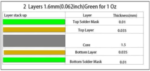
Copper Thickness Considerations in 2-Layer PCB Design Rules
- Standard Copper Thickness: Most 2-layer PCBs use 1 oz (35 µm) copper, suitable for standard current-carrying capacity.
- Heavy Copper: For power applications, 2 oz (70 µm) or more is used to reduce resistance and enhance thermal dissipation.
Dielectric Thickness in 2-Layer PCB Design Rules
- The dielectric thickness affects impedance control and thermal dissipation. Standard 2-layer PCB designs use dielectric thicknesses between 0.1 mm and 0.5 mm depending on performance requirements.
10. Design for Testing (DFT) in 2-Layer PCB Design Rules
To ensure high reliability, 2-layer PCBs should be designed with testability in mind. Incorporating Design for Testing (DFT) principles helps in identifying defects early in the production process.
Test Point Implementation in 2-Layer PCB Design Rules
- Dedicated Test Points: Placing test pads or vias allows easy access for probing during inspection.
- ICT (In-Circuit Testing): Ensures that individual components function correctly before full assembly.
Common PCB Testing Methods in 2-Layer PCB Design Rules
- Flying Probe Testing: Uses moving probes to test connectivity and signal integrity.
- AOI (Automated Optical Inspection): Identifies issues such as misalignment and soldering defects.
- X-Ray Inspection: Used for checking internal layer defects and via connections.
11. Advanced Routing Strategies in 2-Layer PCB Design Rules
Proper routing is critical to maintaining signal integrity and minimizing interference in 2-layer PCBs.
Layer Utilization in 2-Layer PCB Design Rules
- Top Layer: Used for component placement and primary signal routing.
- Bottom Layer: Primarily used for power and ground planes, as well as additional signal routing.
Routing Techniques in 2-Layer PCB Design Rules
- 45-Degree Routing: Helps reduce EMI and improve manufacturability compared to 90-degree turns.
- Differential Pair Routing: Used in high-speed designs for minimizing signal degradation.
- Avoiding Stub Traces: Reduces reflections that can negatively impact signal performance.
12. Environmental Considerations in 2-Layer PCB Design Rules
Sustainability and regulatory compliance are important aspects of 2-layer PCB design rules, particularly for industries requiring environmentally friendly manufacturing.
Lead-Free Soldering in 2-Layer PCB Design Rules
- RoHS Compliance: Ensures that 2-layer PCBs are free from hazardous materials like lead and mercury.
- Alternative Solder Options: Use of lead-free alloys such as SAC305 (Tin-Silver-Copper) for eco-friendly soldering.
Thermal Expansion Management in 2-Layer PCB Design Rules
- CTE (Coefficient of Thermal Expansion): Choosing materials with a CTE matching component packages minimizes thermal stress.
- Use of Thermal Relief Pads: Helps manage localized heating in high-power applications.
13. Common Mistakes in 2-Layer PCB Design Rules and How to Avoid Them
Even experienced designers can encounter errors in 2-layer PCB designs. Below are some frequent mistakes and strategies to prevent them.
Common Errors in 2-Layer PCB Design Rules
- Insufficient Trace Clearance: Can lead to shorts and manufacturing defects. Solution: Maintain at least 6 mil (0.15 mm) clearance.
- Poor Via Placement: Can increase trace lengths and create signal integrity issues. Solution: Place vias near components and optimize via count.
- Improper Grounding: Can cause EMI and noise issues. Solution: Implement a continuous ground plane.
Best Practices to Avoid Design Errors in 2-Layer PCB Design Rules
- Use Design Rule Checks (DRC): Automated checks in PCB design software help detect violations.
- Simulate Signal Integrity: Tools like SPICE or HyperLynx aid in validating circuit performance before fabrication.
- Collaborate with Manufacturers: Ensure that design parameters align with fabrication capabilities.
14. Future Trends in 2-Layer PCB Design Rules
The field of PCB design is evolving, with new technologies and materials enhancing 2-layer PCB performance.
AI-Assisted Design in 2-Layer PCB Design Rules
- AI-powered tools can automate routing decisions, improving layout efficiency and reducing design time.
Flexible 2-Layer PCB Designs
- The use of flexible substrates enables bendable and lightweight PCBs for applications like wearable electronics.
Advanced Materials for High-Performance 2-Layer PCBs
- Graphene and Nanomaterials: Emerging materials promise better conductivity and thermal performance.
15. Conclusion
Designing a 2-layer PCB requires a careful balance between electrical performance, manufacturability, and cost efficiency. By following essential design rules—such as appropriate trace width and spacing, optimal via placement, effective ground plane implementation, and strategic component arrangement—engineers can create reliable and high-performing circuit boards suited for various applications.
While 2-layer PCBs may not offer the same level of complexity as multi-layer designs, they remain a versatile and widely used solution for consumer electronics, industrial control systems, and IoT devices. Proper attention to signal integrity, thermal management, and pcb supplier manufacturability ensures that the final product meets industry standards and performs consistently in real-world conditions.
Understanding 2-layer PCB design rules not only helps in achieving reliable circuits but also improves manufacturability, reduces production costs, and enhances longevity. Whether designing for consumer electronics, automotive applications, or industrial systems, implementing best practices in 2-layer PCB design rules is essential for achieving optimal performance and efficiency.
As PCB technology continues to advance, adhering to 2-layer PCB design rules remains a fundamental aspect of creating high-quality circuit boards that meet the evolving demands of modern electronic applications. For your next PCB project, SQPCB offers top-notch design and manufacturing services to ensure your boards are built to specification and high-quality standards.

Product Center
- long board pcb
- Flexible PCBs
- Special PCB
- Express Printed Circuit Board
- Pcb Prototype
- LED PCB
- PCB
- Printed Circuit Board
- Pcb meaning
- Pcb manufacturer
- Rigid pcb board
- Rigid Flex PCB
Contact Us
 Quote
Quote
 E-mail