Copper PCB Boards: A Comprehensive Guide
Introduction
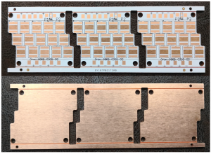
Copper PCB boards are a critical component in modern electronics, offering excellent electrical conductivity, thermal management, and durability. These boards are used across various industries, from consumer electronics to industrial applications. In this article, we explore the types, manufacturing process, advantages, and applications of copper PCB boards.
copper PCB boards.
What is a Copper PCB Board?
A copper PCB board is a printed circuit board that features a copper layer as the primary conductive material. Copper’s high electrical conductivity and heat dissipation capabilities make it the preferred choice for high-performance electronic applications.
Types of Copper PCB Boards
Single-Sided Copper PCB
These boards have a single layer of copper on one side, with components mounted on the other. They are used in simple electronic applications, such as power supplies and household appliances.
Double-Sided Copper PCB
Featuring copper layers on both sides, these PCBs allow for more complex circuit designs and are used in industrial control systems, automotive electronics, and communication devices.
Multilayer Copper PCB
With three or more layers of copper, these PCBs support complex electronic circuits. They are commonly found in medical devices, aerospace electronics, and high-performance computing.
Heavy Copper PCB
Heavy copper PCBs contain thick copper layers (typically above 3 oz per sq ft) and are designed for high-power applications, such as power converters, military electronics, and industrial equipment.
Flexible Copper PCB
Made with flexible substrates, these PCBs are used in applications requiring bending and movement, such as wearable technology, medical sensors, and flexible LED displays.
Manufacturing Process of Copper PCB Boards
Material Selection
Choosing high-quality copper-clad laminates is essential for durability and conductivity.
Circuit Patterning
A conductive copper layer is applied to the substrate, and the circuit pattern is created using photolithography or direct imaging.
Etching Process
Unwanted copper is removed using chemical etching, leaving the desired circuit traces intact.
Drilling
Holes for mounting components and vias are drilled using mechanical or laser drilling.
Plating
A protective layer (such as ENIG, HASL, or OSP) is applied to improve solderability and prevent oxidation.
Solder Mask Application
A solder mask is added to protect the copper traces and prevent short circuits.
Component Assembly
Surface-mount or through-hole components are soldered onto the PCB using automated or manual techniques.
Testing and Quality Control
Electrical testing and inspections ensure the board meets performance and safety standards.
Advantages of Copper PCB Boards
High Electrical Conductivity
Copper has low resistance, ensuring efficient electrical signal transmission.
Excellent Heat Dissipation
Copper’s thermal conductivity helps prevent overheating, improving component lifespan.
Durability and Strength
Copper PCBs are highly resistant to mechanical and environmental stresses.
Compatibility with High-Performance Applications
These boards are ideal for industries requiring reliability and efficiency.
Cost-Effective for High-Volume Production
Mass production of copper PCBs reduces costs while maintaining quality.
Applications of Copper PCB Boards
Consumer Electronics
Used in smartphones, tablets, laptops, and gaming consoles for efficient power management.
Automotive Electronics
Integrated into engine control units, infotainment systems, and safety sensors.
Industrial Power Systems
Essential for high-power converters, motor controllers, and automation systems.
Aerospace and Defense
Used in radar systems, communication devices, and military-grade electronics.
Medical Devices
Found in imaging equipment, diagnostic tools, and wearable health monitors.
Renewable Energy Systems
Key components in solar power inverters and wind energy control circuits.
Choosing the Right Copper PCB Board
Thermal Management Needs
Heavy copper PCBs are recommended for high-power applications requiring superior heat dissipation.
Electrical Performance
The choice of copper thickness and surface finish affects signal integrity and performance.
Application Requirements
Flexible copper PCBs are ideal for dynamic applications, while rigid PCBs are suited for stationary circuits.
Cost Considerations
Balancing material costs with performance requirements ensures cost-effective production.
Conclusion
Copper PCB boards provide unmatched electrical conductivity, durability, and efficiency, making them essential for various industries. Understanding the different types, manufacturing processes, and applications helps in selecting the right PCB for specific needs. As technology advances, copper PCBs continue to drive innovation in modern electronics.

- long board pcb
- Flexible PCBs
- Special PCB
- Express Printed Circuit Board
- Pcb Prototype
- LED PCB
- PCB
- Printed Circuit Board
- Pcb meaning
- Pcb manufacturer
- Rigid pcb board
- Rigid Flex PCB
 Quote
Quote
 E-mail