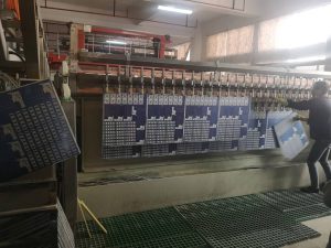
PCB Plating Process: Understanding Electroplating in Circuit Board Manufacturing
Introduction
The PCB plating process, specifically electroplating, is an essential step in printed circuit board (PCB) manufacturing. It enhances the board’s conductivity, reliability, and durability by depositing a thin layer of metal, typically copper, onto the PCB surface and through drilled holes. This ensures strong electrical connections between different layers of the PCB.
This article provides a detailed overview of electroplating in PCB production, including its purpose, types, methods, and process flow.

PCB Plating Process
What is Electroplating in PCB Manufacturing?
Electroplating, also known as metal plating, is a process where a thin layer of metal is deposited onto the PCB surface using an electrolytic solution. This technique is primarily used for:
- Enhancing electrical conductivity
- Protecting against oxidation and corrosion
- Strengthening mechanical durability
- Ensuring robust connections in multi-layer PCBs
Electroplating is crucial for plating through-holes (PTH), vias, and surface pads, ensuring reliable interconnectivity between PCB layers.
Types of PCB Plating Processes
There are several types of plating techniques used in PCB manufacturing:
1. Copper Plating (Electroless and Electroplating)
- Electroless Copper Plating: A chemical process that deposits a thin copper layer on non-conductive surfaces, such as drilled holes, to enable further electroplating.
- Electrolytic Copper Plating: Uses an electric current to deposit copper on PCB traces and vias, ensuring good electrical connectivity.
2. Tin Plating
- Prevents oxidation of copper traces before soldering.
- Acts as a solderable surface for component mounting.
3. Nickel and Gold Plating (ENIG – Electroless Nickel Immersion Gold)
- Provides corrosion resistance and excellent solderability.
- Used for high-reliability applications such as aerospace and medical electronics.
4. Silver Plating
- Improves electrical conductivity and is commonly used in RF and microwave applications.
5. Immersion Gold and Immersion Tin
- Alternative surface finishes that enhance PCB longevity and performance.
PCB Electroplating Process Flow
The electroplating process in PCB manufacturing consists of multiple steps to ensure uniform metal deposition and adhesion. Below is a step-by-step breakdown:
Step 1: PCB Cleaning and Preparation
Before electroplating, the PCB surface must be cleaned to remove contaminants such as dust, oil, or oxidation. This step ensures proper metal adhesion.
- Chemical Cleaning: Uses acid-based solutions to clean the copper surface.
- Micro-etching: Removes a thin layer of copper oxide to improve plating adhesion.
Step 2: Drilling and Desmearing
- Drilling: Holes for vias and through-hole components are drilled into the PCB.
- Desmearing: Removes debris and resin residue left after drilling, ensuring a clean surface for plating.
Step 3: Electroless Copper Deposition (For PTH Vias)
A thin layer of copper is chemically deposited in the drilled holes to make them conductive, preparing them for electroplating.
Step 4: Electrolytic Copper Plating
This step deposits additional copper onto the PCB surface and through-holes:
- PCBs are submerged in an electrolytic bath containing copper sulfate solution.
- An electric current is applied, attracting copper ions to conductive areas.
- A controlled layer of copper (usually 25-50 microns) is deposited.
Step 5: Surface Finish Plating (Optional)
Depending on the PCB design and application, additional plating layers may be applied:
- Nickel and gold (ENIG) for high-reliability applications.
- Tin plating for improved solderability.
- Silver or palladium for specialized uses.
Step 6: Plating Inspection and Quality Control
- Thickness Measurement: Ensures uniform copper deposition.
- Cross-Section Analysis: Examines plated through-holes to detect defects.
- Adhesion Testing: Verifies the metal layer’s bonding strength.
- Electrical Testing: Confirms conductivity and proper interconnections.
Key Considerations in PCB Electroplating
1. Plating Thickness Control
- Too thin: Weak conductivity and mechanical instability.
- Too thick: Increased production costs and potential PCB warping.
2. Uniformity of Metal Deposition
- Uneven plating can cause electrical failures and mechanical stress.
- Agitation methods and bath chemistry must be optimized.
3. Environmental Regulations
- Wastewater from electroplating contains heavy metals that require proper treatment.
- Many manufacturers adopt eco-friendly lead-free and ROHS-compliant plating solutions.
4. Compatibility with PCB Design Requirements
- Different surface finishes (e.g., ENIG, immersion tin) are selected based on application needs, cost, and solderability.
- RF/microwave circuits may require specialized silver or gold plating.
Advantages of PCB Electroplating
- Improved Electrical Performance – Enhances conductivity and reduces signal loss.
- Increased Durability – Protects against oxidation, wear, and corrosion.
- Enhanced Solderability – Ensures better component attachment.
- Stronger Mechanical Integrity – Supports multi-layer PCB connectivity.
- Scalability in Mass Production – Electroplating is suitable for high-volume manufacturing.
Future Trends in PCB Plating Technology
1. Advanced Surface Finishes
- Lead-free and ROHS-compliant plating materials are becoming industry standards.
- Hybrid plating solutions enhance PCB longevity.
2. Nanotechnology-Based Plating
- Nano-coatings improve thermal and electrical performance.
- Helps in miniaturized electronic devices.
3. AI-Driven Plating Process Optimization
- Artificial intelligence is used to monitor and control electroplating quality.
- Automated defect detection improves manufacturing precision.
4. Eco-Friendly Plating Techniques
- Water-based electroplating minimizes environmental impact.
- Recyclable plating chemicals reduce hazardous waste.
Conclusion
The PCB plating process plays a crucial role in enhancing conductivity, solderability, and durability. Electroplating techniques such as copper plating, nickel-gold (ENIG), tin plating, and immersion finishes ensure that PCBs function reliably across consumer electronics, automotive, aerospace, and industrial applications.
With advancements in nanotechnology, AI-driven optimization, and sustainable plating solutions, the future of PCB electroplating continues to evolve, promising higher efficiency, lower environmental impact, and improved electronic performance. Understanding the PCB plating process is essential for engineers and manufacturers aiming to produce high-quality, long-lasting circuit boards.
- long board pcb
- Flexible PCBs
- Special PCB
- Express Printed Circuit Board
- Pcb Prototype
- LED PCB
- PCB
- Printed Circuit Board
- Pcb meaning
- Pcb manufacturer
- Rigid pcb board
- Rigid Flex PCB

 Quote
Quote
 E-mail