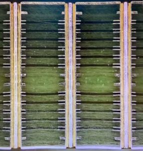
Multi Layer Circuit Boards: The Backbone of Modern Electronics
Introduction
Multi layer circuit boards (MLBs) are a crucial component in the electronics industry, playing a vital role in the functionality and performance of various electronic devices. These circuit boards, consisting of multiple layers of conductive and insulating materials, enable more complex and compact designs, making them indispensable for modern electronic applications. In this article, we will explore the structure, benefits, applications, and manufacturing process of multi-layer circuit boards.

Multi-Layer Circuit Boards
What is a Multi-Layer Circuit Board?
A multi-layer circuit board is a printed circuit board (PCB) with more than two layers of conductive material. Unlike single-layer and double-layer PCBs, multi-layer PCBs have three or more layers, which are laminated together with insulating materials in between. The additional layers allow for more intricate circuit designs, higher component density, and improved performance.
The typical structure of a multi-layer PCB includes:
- Core: A solid dielectric material that provides structural support.
- Conductive Layers: Copper traces that form the circuit connections.
- Prepreg (Pre-impregnated Composite Fibers): Insulating layers that separate the conductive layers and provide electrical insulation.
- Via Holes: Holes that connect different layers, allowing electrical signals to pass through.
- Solder Mask and Silkscreen: The outermost layers that protect the board and provide labeling.
Advantages of Multi-Layer Circuit Boards
1. Higher Circuit Density
One of the primary benefits of multi-layer PCBs is their ability to accommodate a higher circuit density within a compact size. By stacking multiple layers, designers can create more complex circuits without increasing the board’s footprint.
2. Improved Signal Integrity
Multi-layer PCBs provide better signal integrity and reduced electromagnetic interference (EMI). The close proximity of power and ground planes helps in minimizing noise and improving signal transmission, making them ideal for high-speed applications.
3. Enhanced Durability and Reliability
Due to their layered structure, multi-layer PCBs are more robust and durable compared to single-layer and double-layer PCBs. The lamination process enhances mechanical strength and prevents warping, making them suitable for high-performance and rugged environments.
4. Reduced Size and Weight
Multi-layer PCBs allow for miniaturization, which is essential for modern electronic devices such as smartphones, medical implants, and wearables. The compact design reduces weight while maintaining high functionality.
5. Better Heat Dissipation
Efficient thermal management is crucial for electronic devices. Multi-layer PCBs distribute heat more effectively, preventing overheating and extending the lifespan of components.
Applications of Multi-Layer Circuit Boards
Multi-layer PCBs are widely used in various industries due to their high performance and reliability. Some key applications include:
1. Consumer Electronics
Smartphones, tablets, laptops, and gaming consoles rely on multi-layer PCBs for their compact and complex circuit designs. These boards enable high-speed data processing and efficient power distribution.
2. Medical Devices
Medical equipment such as MRI machines, pacemakers, and diagnostic tools require reliable and high-precision PCBs. Multi-layer boards provide stability and accuracy, ensuring optimal performance in critical healthcare applications.
3. Automotive Industry
Modern vehicles incorporate advanced electronic systems, including GPS, entertainment systems, engine control units (ECUs), and safety features. Multi-layer PCBs enhance these systems’ efficiency and reliability, contributing to vehicle automation and smart features.
4. Aerospace and Defense
Aerospace and defense applications demand highly durable and reliable PCBs that can withstand extreme conditions. Multi-layer PCBs are used in radar systems, communication devices, and avionics, ensuring high performance and longevity.
5. Industrial Equipment
Multi-layer PCBs play a significant role in industrial automation, robotics, and power control systems. Their high reliability and durability make them ideal for manufacturing and automation applications.
Manufacturing Process of Multi-Layer Circuit Boards
The manufacturing of multi-layer PCBs involves several intricate steps to ensure quality and functionality. The process includes:
1. Design and Layout
The first step involves designing the PCB layout using specialized CAD software. Designers define the circuit patterns, component placements, and layer arrangements.
2. Material Selection
Choosing the right materials is critical for performance and reliability. The core material, prepreg, and copper foils are selected based on the application’s requirements.
3. Lamination and Layering
The multiple layers of conductive and insulating materials are stacked and laminated under high temperature and pressure. This process ensures strong bonding and alignment.
4. Drilling and Plating
Holes (vias) are drilled to connect different layers. The drilled holes are then plated with conductive materials, ensuring electrical continuity between layers.
5. Etching and Circuit Formation
The unwanted copper is etched away, leaving behind the required circuit patterns. This process is done using chemical solutions and photolithography techniques.
6. Solder Mask and Silkscreen Application
A solder mask is applied to protect the copper traces from oxidation and short circuits. Silkscreen printing is then used to label components and provide reference markings.
7. Testing and Quality Control
Each PCB undergoes rigorous testing, including electrical testing, visual inspection, and functional testing. This ensures that the board meets industry standards and specifications.
8. Final Assembly and Packaging
The finished PCBs are assembled with components, tested again, and packaged for shipment to customers.
Conclusion
Multi-layer circuit boards have revolutionized the electronics industry, enabling the development of sophisticated and compact devices. Their high circuit density, enhanced reliability, and improved signal integrity make them indispensable in consumer electronics, medical devices, automotive systems, aerospace, and industrial applications. As technology continues to evolve, multi-layer PCBs will remain at the forefront of innovation, driving the future of electronics.
- long board pcb
- Flexible PCBs
- Special PCB
- Express Printed Circuit Board
- Pcb Prototype
- LED PCB
- PCB
- Printed Circuit Board
- Pcb meaning
- Pcb manufacturer
- Rigid pcb board
- Rigid Flex PCB

 Quote
Quote
 E-mail