Phototool Films for PCB Exposure: Importance, Types, and Best Practices
Introduction
In PCB (Printed Circuit Board) manufacturing, phototool films play a crucial role in the exposure process, ensuring the accurate transfer of circuit patterns onto photoresist-coated layers. These films act as high-precision masks, blocking or allowing UV light to pass through specific areas, thereby defining the circuit layout with extreme accuracy.
With the rise of high-density interconnect (HDI) and fine-line PCBs, the quality of phototool films directly impacts alignment precision, resolution, and overall yield. Selecting the right phototool material, thickness, and processing conditions is essential to achieve optimal circuit definition and defect-free PCB production.
This article explores the role of phototool films in PCB exposure, types of films, processing techniques, advantages, limitations, and best practices to ensure high-precision circuit imaging.
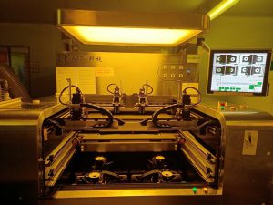
Phototool Films
The Role of Phototool Films in PCB Exposure
During the PCB exposure process, phototool films are placed over photoresist-coated PCB layers. When exposed to UV light, the phototool controls the areas that are polymerized or washed away, thereby defining the circuit pattern.
Functions of Phototool Films
- Precise Circuit Pattern Transfer – Ensures accurate light blocking or transmission for high-resolution imaging.
- Alignment and Registration Accuracy – Maintains correct positioning for multilayer PCBs.
- Consistency and Repeatability – Enables mass production of consistent PCBs with minimal variation.
- Prevention of Light Scattering – Ensures sharp circuit edges and prevents overexposure or underexposure.
Types of Phototool Films Used in PCB Exposure
1. Silver Halide Film
- Commonly used in traditional PCB manufacturing.
- High contrast and fine resolution suitable for fine-pitch designs.
- Sensitive to humidity and scratches, requiring careful handling.
- Best for inner and outer layer exposure.
2. Diazo Film
- Cost-effective and durable, but lower contrast compared to silver halide.
- Suitable for general PCB applications with moderate resolution needs.
- Requires longer exposure times.
3. Photoplotter Film (Laser Plotted Film)
- Produced using computer-controlled laser photoplotters.
- Extremely high resolution and accuracy for HDI and fine-line PCBs.
- Provides dimensional stability and excellent registration control.
4. Polyester-Based Phototool Films
- Designed for repeated use in high-volume PCB manufacturing.
- Stronger mechanical properties, reducing risks of tearing or stretching.
- Suitable for long production cycles and multi-layer PCB alignment.
Phototool Film Processing Techniques
1. Film Preparation and Handling
- Films should be stored in a humidity-controlled, dust-free environment.
- Gloves must be worn to prevent contamination and fingerprints.
- Proper cutting and alignment ensure accurate positioning on PCBs.
2. Exposure Process
- The phototool film is placed on the photoresist-coated PCB surface.
- UV light exposure hardens the photoresist in areas not blocked by the film.
- Alignment accuracy is critical for double-sided and multilayer PCBs.
3. Development and Etching
- After exposure, the PCB is developed, removing unexposed photoresist.
- The exposed areas of the copper layer are etched, forming the circuit pattern.
- The phototool film is removed and can be reused for consistent production.
Advantages and Limitations of Phototool Films
✅ Advantages
- High Precision and Fine-Line Resolution – Supports micron-level accuracy for HDI PCBs.
- Reusable for Multiple Exposures – Reduces material costs in mass production.
- Cost-Effective for Small to Mid-Scale Production – Lower initial investment compared to direct imaging (DI) exposure.
- Compatible with Various Photoresist Materials – Works well with dry film and liquid photoresists.
❌ Limitations
- Mechanical Wear Over Time – Repeated use may lead to scratches or distortion, affecting pattern accuracy.
- Dimensional Stability Issues – Thermal expansion and humidity variations can cause slight misalignment in multilayer PCBs.
- Requires High-Precision Handling – Any misalignment or dust contamination can cause exposure defects.
- Limited for Ultra-High Volume Production – Direct imaging (DI) is often preferred for scaling up production due to higher speed and automation.
Best Practices for Using Phototool Films in PCB Manufacturing
- Ensure Clean and Controlled Storage
- Store films at consistent temperature (20–25°C) and humidity (50% RH).
- Keep them in protective sleeves to avoid scratches or dust contamination.
- Use High-Resolution Films for Fine-Line PCBs
- For high-density circuits (below 50 µm line width), laser photoplotter films are recommended.
- Lower-resolution diazo films can be used for general PCB applications.
- Regularly Check Film Alignment and Registration
- Before each exposure, inspect films for distortion, warping, or damage.
- Align phototool films precisely using fiducial marks and registration holes.
- Optimize UV Exposure Settings
- Calibrate exposure time, intensity, and distance to achieve optimal photoresist hardening.
- Avoid overexposure or underexposure, which can lead to circuit defects.
- Monitor Film Usage and Replace When Necessary
- Replace phototool films after multiple uses or visible wear.
- Regular maintenance of exposure units ensures consistent imaging quality.
Future Trends: Transition to Direct Imaging (DI) Exposure
While phototool films remain widely used, the industry is gradually shifting toward Direct Imaging (DI) exposure, which offers:
- Higher automation and speed
- No need for physical films, reducing alignment errors
- Better scalability for high-volume production
However, phototool films continue to be preferred in many cost-sensitive PCB production lines, particularly for standard multilayer PCBs and mid-volume manufacturing.
Conclusion
Phototool films are essential materials in PCB exposure, playing a crucial role in accurate circuit pattern transfer, registration control, and production efficiency. By selecting the right film type, ensuring proper handling, and optimizing exposure settings, PCB manufacturers can achieve high-quality imaging and defect-free circuits.
While Direct Imaging (DI) technology is emerging as a next-generation alternative, phototool films remain a reliable and cost-effective solution for many PCB manufacturing applications. Implementing best practices in film maintenance, alignment control, and exposure optimization will help ensure high-precision, repeatable results in PCB production.

- long board pcb
- Flexible PCBs
- Special PCB
- Express Printed Circuit Board
- Pcb Prototype
- LED PCB
- PCB
- Printed Circuit Board
- Pcb meaning
- Pcb manufacturer
- Rigid pcb board
- Rigid Flex PCB
 Quote
Quote
 E-mail