Flash gold PCB plating is a surface treatment process that applies a thin layer of gold onto the circuit board’s copper traces using an electroplating technique. This method, also known as pre-gold plating, provides good conductivity, wear resistance, and oxidation protection while being more cost-effective than full electroplated gold.
The term “flash gold” comes from the English word “Flash,” meaning quick or thin gold plating. It is widely used in consumer electronics, industrial devices, and PCB connectors, where moderate conductivity and affordability are required.
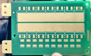
flash gold PCB
How Flash Gold PCB Plating Works
Flash gold plating is performed by immersing the PCB into a nickel-gold electroplating bath, where a thin layer of gold is deposited onto the nickel layer under an electrical current. This method allows for faster processing and lower gold consumption, making it an economical alternative to full electroplated hard gold.
- Nickel Plating: A nickel layer is first applied as a barrier between the copper and gold. This prevents electron migration and diffusion between the two metals.
- Gold Flashing: A thin gold layer is electroplated onto the nickel to enhance conductivity and prevent oxidation.
- Final Processing: The plated PCB undergoes cleaning, inspection, and quality testing before assembly.
Flash gold plating is often used as a pre-treatment step for hard gold plating, but some manufacturers use it as a final surface treatment for cost-saving purposes.
Characteristics of Flash Gold PCB Plating
Flash gold PCB plating has distinct features that make it suitable for certain applications:
- Thin Gold Layer: The gold layer is thinner than that of traditional electroplated nickel-gold, making it a cost-effective solution.
- Good Conductivity: Provides stable electrical performance suitable for moderate-power circuits.
- Wear Resistance: Offers some durability but is less resistant to friction than fully electroplated gold.
- Oxidation Protection: Helps prevent oxidation and corrosion but may not be as long-lasting as ENIG or full hard gold plating.
- Low Cost: Compared to other gold-plating methods, flash gold is a budget-friendly option for non-critical applications.
Applications of Flash Gold PCB Plating
Flash gold is commonly used in low to mid-range electronic products, where cost efficiency and basic gold-plated surface performance are required.
- Consumer Electronics: Used in smartphones, laptops, and home appliances where moderate conductivity and oxidation resistance are needed.
- PCB Connectors & Edge Contacts: Applied to connector surfaces and gold fingers that require limited wear resistance.
- Industrial Electronics: Utilized in low-cost circuit boards that require some anti-corrosion properties.
- Budget PCBs: Suitable for mass-produced circuit boards where full hard gold plating is too expensive.
Advantages of Flash Gold PCB Plating
Flash gold offers several benefits, making it an attractive option for cost-sensitive applications:
- Lower Cost: Requires less gold than traditional hard gold plating, reducing material expenses.
- Fast Processing Time: The electroplating process is quick and efficient, enabling high-volume PCB production.
- Basic Corrosion Protection: Provides oxidation resistance, extending PCB lifespan in low-wear environments.
- Good Conductivity: Ensures consistent electrical performance, suitable for standard circuit board designs.
Disadvantages of Flash Gold PCB Plating
While flash gold is a cost-effective solution, it does have some limitations:
- Thin Gold Layer: The gold coating is relatively thin, making it less durable compared to hard gold or ENIG.
- Limited Wear Resistance: Not suitable for high-friction applications, such as frequently used connectors.
- Shorter Shelf Life: PCBs with flash gold plating may experience oxidation over time, affecting solderability and reliability.
- Lower Thickness Control: The thin layer may not fully cover the nickel beneath, leading to potential oxidation.
Due to these drawbacks, flash gold plating is not recommended for high-performance electronics, military applications, or PCBs requiring long-term durability.
Flash Gold PCB Plating vs. Other Gold Plating Methods
There are several gold plating techniques used in PCB manufacturing, and it’s important to compare flash gold with other options:
- Hard Gold Plating (Electroplated Nickel-Gold):
- Thicker gold layer, higher durability, and better wear resistance.
- Used in high-friction applications like gold fingers and PCB connectors.
- More expensive than flash gold.
- Soft Gold Plating (Pure Gold Electroplating):
- Pure gold layer, softer but provides better wire bonding capability.
- Used in COB (Chip-on-Board) and BGA substrates.
- ENIG (Electroless Nickel Immersion Gold):
- Flat surface finish, suitable for fine-pitch components.
- More oxidation-resistant and widely used in high-reliability electronics.
- More expensive than flash gold, but offers better shelf life and solderability.
Flash gold is mainly chosen for cost savings, but ENIG, hard gold, and soft gold plating are preferred for applications requiring better reliability, durability, and performance.
Conclusion
Flash gold PCB plating is a cost-effective surface treatment that provides basic conductivity and oxidation resistance while using minimal gold material. It is commonly used in budget-friendly electronics, connectors, and consumer devices but is not suitable for high-wear or long-term reliability applications.
For high-performance PCBs, ENIG, hard gold, or soft gold plating are preferred due to better durability and conductivity. However, when affordability and quick production are the priority, flash gold remains a practical option for PCB manufacturers.
If you need custom PCB surface treatments, Shuoqiang Electronics offers cost-effective flash gold PCBs and advanced plating solutions to meet your product requirements. Contact us today for professional PCB manufacturing services!
our linkedin sqpcb.com

- long board pcb
- Flexible PCBs
- Special PCB
- Express Printed Circuit Board
- Pcb Prototype
- LED PCB
- PCB
- Printed Circuit Board
- Pcb meaning
- Pcb manufacturer
- Rigid pcb board
- Rigid Flex PCB
 Quote
Quote
 E-mail