I. Importance of Advanced PCBs in Modern Electronics
1. The Cornerstone of Electronic Products
Advanced printed circuit board (PCBs) are essential in powering modern electronics, ranging from IoT devices to aerospace applications. Acting as the backbone of devices, PCBs provide the necessary physical support and electrical connections for components to work seamlessly. In applications like automotive PCBs, these advanced solutions integrate processors, sensors, and communication modules to enable cutting-edge functionalities such as ADAS (Advanced Driver Assistance Systems).
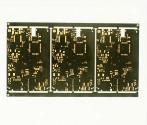
Advanced printed circuit board
2. Driving Miniaturization and High Performance
The demand for smaller, more powerful devices has led to innovations like high-density PCBs, HDI technology, and multilayer PCBs. These advancements allow for compact designs without sacrificing performance, particularly in flexible PCBs and rigid-flex PCBs, which are widely used in wearable devices and aerospace equipment where size and durability are critical.
3. Ensuring Signal Integrity and Thermal Management
In high-speed digital and high-frequency PCBs, maintaining PCB signal integrity is essential for proper performance. Features like impedance control, optimized advanced circuit board layout, and effective thermal management ensure reliable operation even under demanding conditions. These capabilities are particularly crucial for medical PCBs and aerospace PCBs, where precision and reliability are non-negotiable.
II. Production Process Insights
1. Design Stage
Schematic Design and Advanced PCB Features
The first step involves creating a detailed electrical schematic that accounts for PCB customization and advanced electronic circuits. Components are carefully selected during this stage, considering PCB material selection to ensure performance and durability in various applications.
Layout Planning and Signal Optimization
During the layout phase, emphasis is placed on optimizing PCB signal integrity through proper trace routing and impedance control. The use of advanced substrate materials like Rogers laminates ensures minimal signal loss in high-frequency PCBs.
Wiring and Layer Management
Modern PCB stack-ups often include multilayer PCBs to handle complex wiring. Vias and HDI technology, including microvias, are utilized to connect layers efficiently and maintain high performance in high-density PCBs.
2. Manufacturing Stage
Substrate Material Selection
The choice of substrate impacts both performance and cost. For example:
-
FR-4: Versatile for general applications.
-
Advanced Substrate Materials: Essential for aerospace PCBs and IoT PCBs requiring high-frequency operation.
Pattern Transfer and PCB Fabrication Process
High-resolution photolithography techniques are employed to create precise circuit patterns. This step is critical for achieving the fine details required in high-density PCBs.
Etching and Drilling
Etching removes excess copper to form the circuit pattern, while precise drilling supports PCB assembly techniques and ensures compatibility with PCB industry standards.
Solder Mask and Legend Printing
A solder mask protects the circuitry, while legend printing provides essential assembly instructions, enhancing the efficiency of PCB assembly techniques.
III. Quality Control and Challenges
1. Key Points of Quality Control
PCB Testing Methods
Comprehensive testing ensures functionality and reliability. This includes:
-
Continuity Testing: Ensures all traces are properly connected.
-
Impedance Testing: Confirms signal integrity in high-frequency PCBs.
-
Environmental Testing: Simulates real-world conditions for high-performance PCBs.
Sustainable PCB Manufacturing Practices
With rising environmental concerns, manufacturers are adopting sustainable PCB manufacturing processes. This includes using eco-friendly materials and recycling byproducts from the PCB fabrication process.
2. Challenges
Meeting Industry Standards
Adhering to PCB industry standards, such as IPC and RoHS, ensures safety, performance, and environmental compliance.
Keeping Pace with Technological Advances
The rapid evolution of electronics requires continuous innovation in areas like rapid PCB prototyping, IoT PCBs, and medical PCBs to remain competitive.
IV. Applications of Advanced PCBs
1. Automotive Electronics
Automotive PCBs enable complex functionalities like collision avoidance systems, EV battery management, and infotainment systems. Their reliability is critical in harsh operating conditions.
2. Aerospace
Aerospace PCBs withstand extreme environments and are integral to avionics, satellite systems, and radar technologies.
3. Medical Devices
From imaging equipment to wearable health monitors, medical PCBs support precision and reliability essential for healthcare innovation.
4. IoT and Consumer Electronics
IoT PCBs power connected devices, enabling seamless communication and smart functionality in everything from home automation systems to industrial sensors.
V. Advancements in PCB Technology
1. HDI Technology and Microvias
HDI technology enables high-performance designs with fine lines and compact features, essential for high-density and high-speed applications.
2. Flexible and Rigid-Flex PCBs
These designs combine flexibility with durability, making them ideal for applications requiring both movement and structural stability.
3. Advanced Materials for High-Frequency PCBs
Using advanced substrate materials, such as PTFE, ensures reliable performance in high-speed and high-frequency applications.
VI. Conclusion
Advanced PCBs are the foundation of modern electronics, enabling innovation across industries. From multilayer PCBs to IoT PCBs, their integration drives performance, reliability, and sustainability. By adopting sustainable PCB manufacturing practices and leveraging advancements like HDI technology, businesses can stay ahead in an ever-evolving technological landscape. Investing in cutting-edge PCB manufacturing and design ensures success in creating high-performance electronic solutions.
linkedin https://www.linkedin.com/feed/update/urn:li:activity:
7097167729337532416/

- long board pcb
- Flexible PCBs
- Special PCB
- Express Printed Circuit Board
- Pcb Prototype
- LED PCB
- PCB
- Printed Circuit Board
- Pcb meaning
- Pcb manufacturer
- Rigid pcb board
- Rigid Flex PCB
 Quote
Quote
 E-mail