Circuit Board Manufacturing: In today’s fast-evolving technological landscape, Printed Circuit Boards (PCBs) serve as the backbone of modern electronics. Found in everything from smartphones and computers to industrial machines and automotive systems, PCBs are indispensable to the functionality of nearly all electronic devices. Their ability to provide seamless electrical connections and mechanical support makes them one of the most critical components in electronics manufacturing.
Circuit Board Manufacturing
What Is a Circuit Board?
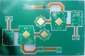
A circuit board, commonly known as a Printed Circuit Board (PCB), is a flat, non-conductive board that provides mechanical support and electrical connections for electronic components. It acts as the “nervous system” of an electronic device, enabling the transmission of signals and power across various components.
Key Components of a Circuit Board
- Base Material: Typically made from fiberglass-reinforced epoxy resin (FR4), the base provides structural stability.
- Conductive Pathways: Thin layers of copper form the conductive traces that connect various components.
- Mounted Components: Resistors, capacitors, diodes, and integrated circuits (ICs) are mounted on the PCB to perform specific functions.
The combination of these elements creates a highly integrated system capable of powering the most complex electronic devices.
The Circuit Board Manufacturing Process
The journey of creating a functional PCB involves multiple precise and intricate steps. Each stage is critical to ensuring the board’s performance and reliability.
1. Design and Layout
The manufacturing process begins with designing the PCB. Engineers use advanced software like Altium Designer, Eagle, or KiCad to map out the board’s circuitry. This digital blueprint defines:
- The placement of components.
- The routing of conductive traces to ensure signal integrity and minimize interference.
- The number of layers required for complex designs.
Once finalized, the design is converted into Gerber files, which serve as instructions for manufacturing machines.
2. Material Preparation
The base material, usually fiberglass (FR4) or a metal core for specific applications, is laminated with a thin copper layer. This copper-clad board will eventually become the foundation for the circuit pathways.
3. Etching and Layering
- A photosensitive resist is applied to the copper-clad board.
- The board is exposed to ultraviolet (UV) light, transferring the circuit design onto the material. Unwanted copper is then removed through an etching process, leaving only the desired traces.
- For multi-layer PCBs, additional layers are added, aligned, and bonded together under heat and pressure.
4. Drilling and Plating
Precision drilling creates small holes (vias) that allow electrical connections between layers or components. These holes are plated with conductive material, ensuring signal continuity across the board.
5. Solder Mask Application
A protective solder mask is applied to insulate the copper traces and prevent accidental soldering during component assembly. This layer is typically green, although other colors are available.
6. Silkscreening
The final step in manufacturing involves printing component identifiers, logos, or other markings on the PCB. This silkscreen layer aids assembly technicians in placing components accurately.
7. Testing and Quality Control
Before proceeding to assembly, the PCB undergoes rigorous testing, including:
- Automated Optical Inspection (AOI): Detects defects in trace alignment or component placement.
- Electrical Testing: Ensures all circuits are functional and free from shorts or open connections.
- X-Ray Testing: Examines internal layers in multi-layer boards.
PCB Assembly: Bringing the Circuit Board to Life
Once the PCB is manufactured, the next step is assembly, where electronic components are mounted to bring the board to life. Modern assembly processes use high-precision automation to ensure speed, accuracy, and efficiency.
Methods of PCB Assembly
- Surface Mount Technology (SMT):
- Components are placed directly onto the board’s surface.
- Highly efficient for compact designs and high-density PCBs.
- Automated machines precisely position components, which are then secured through a reflow soldering process.
- Through-Hole Technology (THT):
- Components with leads are inserted into pre-drilled holes and soldered on the opposite side.
- Preferred for components requiring mechanical strength, such as connectors or power supplies.
Hybrid PCBs often use both SMT and THT, combining their advantages to optimize performance and reliability.
Soldering Techniques
- Reflow Soldering: Used for SMT components, this process involves heating solder paste to create secure electrical and mechanical connections.
- Wave Soldering: Common for THT components, where the board passes over a wave of molten solder to attach leads to the PCB.
Final Testing and Inspection
After assembly, the board undergoes extensive testing to ensure quality and functionality:
- Functional Testing: Verifies that the PCB performs as intended in real-world conditions.
- AOI and X-Ray Inspections: Detect soldering defects and ensure proper component placement.
Applications of PCBs
PCBs are integral to countless industries, powering a wide range of devices and systems:
- Consumer Electronics: Smartphones, tablets, laptops, and gaming consoles rely on compact, multi-layer PCBs to enable their advanced features.
- Automotive Electronics: Modern vehicles use PCBs for systems like engine control units (ECUs), advanced driver-assistance systems (ADAS), and in-car entertainment.
- Industrial Machines: PCBs ensure efficient operation in robotics, automation equipment, and control systems.
- Medical Devices: Life-critical devices such as pacemakers, diagnostic equipment, and imaging systems depend on high-precision, reliable PCBs.
- Telecommunications: From 5G base stations to data centers, PCBs are vital for high-speed signal processing and networking.
Emerging Trends in Circuit Board Manufacturing and Assembly
The PCB industry continues to evolve, driven by advancements in technology and increasing market demands. Key trends include:
1. Miniaturization
As devices become smaller and more powerful, the demand for compact, high-density PCBs with multi-layer and flexible designs continues to rise.
2. Eco-Friendly Practices
With growing environmental concerns, manufacturers are adopting lead-free materials, recyclable substrates, and energy-efficient processes to reduce their ecological footprint.
3. Automation and Industry 4.0
Smart manufacturing techniques, including AI-driven design tools and real-time production monitoring, are enhancing efficiency and quality in PCB production.
4. High-Frequency PCBs
The rise of 5G networks and IoT devices is driving the need for PCBs that can handle high-speed, high-frequency signals without signal degradation.
Conclusion
Printed Circuit Boards (PCBs) are the foundation of modern electronic devices, providing both structural support and seamless electrical connectivity. From initial design to final assembly, every step in the PCB manufacturing and assembly process demands precision, innovation, and quality assurance.
As a PCB manufacturer, our focus remains on staying ahead of industry trends, adopting cutting-edge technologies, and delivering reliable, high-performance solutions. Whether for consumer electronics, automotive systems, or medical devices, we are committed to meeting the evolving needs of our customers and driving the future of electronic innovation.
linkedin sqpcb.com

- long board pcb
- Flexible PCBs
- Special PCB
- Express Printed Circuit Board
- Pcb Prototype
- LED PCB
- PCB
- Printed Circuit Board
- Pcb meaning
- Pcb manufacturer
- Rigid pcb board
- Rigid Flex PCB
 Quote
Quote
 E-mail