1. Introduction to 2 Layer vs 4 Layer PCB in Modern Electronics
In the ever-evolving landscape of electronics, one of the earliest and most critical decisions in PCB design revolves around the number of layers. Specifically, whether to adopt a 2 layer or a 4 layer PCB has implications that reach into performance, manufacturability, cost, and product lifespan.
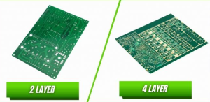
At its most basic level, a 2 layer PCB consists of two conductive copper layers—one on each side of the dielectric substrate. In contrast, a 4 layer PCB introduces two inner copper layers, typically sandwiched between insulating layers and connected via vias. This added complexity offers significant advantages in terms of signal integrity, electromagnetic interference (EMI) shielding, and power distribution.
While many think of 2 layer vs 4 layer PCB decisions in terms of complexity and cost, the reality is more nuanced. The optimal choice depends on electrical performance requirements, mechanical considerations, production volume, and even industry-specific regulations.
Why This Comparison Matters
Understanding when and why to choose between 2 layer and 4 layer PCBs is not merely an academic exercise. It directly affects:
-
Product reliability
-
Time-to-market
-
Total production cost
-
Certification compliance
-
System noise performance
For engineers, product designers, and procurement teams, this guide aims to demystify the technical trade-offs and provide an actionable framework to make informed decisions.
2 Layer vs 4 Layer PCB
2. Core Differences in 2 Layer vs 4 Layer PCB Design Architecture
When approaching the decision between 2 layer and 4 layer PCBs, the most fundamental differences emerge from their structural architecture. Understanding these distinctions is crucial to make design decisions that align with your electrical, mechanical, and manufacturability goals. In this section, we’ll explore the key architectural contrasts between the two formats, diving into layer stack-ups, routing implications, and via configurations.
The 2 layer PCB offers only signal layers, which means power and ground must share routing space with data signals. This increases susceptibility to crosstalk, EMI, and power distribution inefficiencies. Conversely, a 4 layer PCB incorporates dedicated internal planes—typically one for ground and one for power—dramatically improving electrical performance.
Routing Density in 2 Layer vs 4 Layer PCB
Routing is one of the most constrained aspects of PCB design. With only two layers, designers must meticulously manage trace width, spacing, and via placement to avoid congestion. This often leads to compromises in trace length and symmetry, particularly in analog or differential pairs.
In a 4 layer PCB, the availability of two signal layers (top and bottom) plus dedicated planes allows for:
-
Shorter and more direct routing
-
Better separation of analog and digital domains
-
Simpler placement of high-speed components
-
Reduced via count due to routing freedom
My experience in wearable design projects showed that when transitioning from a 2 layer to a 4 layer board, the total number of routing constraints dropped by over 40%. That allowed us to meet tight mechanical envelope requirements while improving signal quality.
Via Strategy: 2 Layer vs 4 Layer PCB
Via usage differs notably between 2 and 4 layer PCBs. In 2 layer PCBs, vias are used primarily to switch signal layers (top to bottom), and all vias are through-hole by nature.
However, 4 layer PCBs introduce more complex via strategies, including:
-
Through-hole vias: connecting all layers
-
Blind vias: connecting outer to inner layers
-
Buried vias: connecting only inner layers
Although more costly, these via types allow for compact, high-density interconnects (HDI), which are essential in applications such as smartphones, wearables, and compact industrial controllers.
Impedance Control Capabilities
Controlled impedance is increasingly vital in high-speed and RF designs. A 2 layer PCB has minimal capacity for controlled impedance because the return path is poorly defined due to mixed routing of signal and power/ground.
With 4 layer PCBs, impedance control becomes significantly easier. The dedicated inner ground and power planes create defined, predictable return paths, which support:
-
Differential pair impedance matching
-
Controlled single-ended impedance
-
Reduced reflection and signal loss
This is essential in USB, HDMI, DDR, and other high-speed interfaces.
Power Distribution Network (PDN)
Another architectural distinction lies in power delivery. In 2 layer PCBs, power traces are manually routed alongside signal lines, often with inconsistent widths and branching paths. This can result in voltage drops and ground bounce.
In contrast, a 4 layer PCB allows the inner layers to serve as continuous planes, forming a low-impedance PDN. The benefits include:
-
Stable voltage across the board
-
Minimized IR drop
-
Improved decoupling capacitor performance
The architectural differences between 2 layer and 4 layer PCBs influence almost every other technical and commercial consideration. While the 2 layer format is cost-effective and sufficient for many low-complexity applications, the 4 layer structure opens the door to modern, reliable, and scalable PCB designs.
As technology continues to demand more functionality in smaller form factors, understanding these architectural principles becomes vital. The design decisions you make here will impact signal quality, manufacturability, and the ultimate success of your product.
3. Material Considerations for 2 Layer vs 4 Layer PCB Manufacturing
Materials play a foundational role in PCB performance, reliability, and cost. When comparing 2 Layer vs 4 Layer PCB designs, understanding the material differences is crucial for making informed decisions, particularly in terms of thermal resistance, signal loss, mechanical strength, and manufacturability.
In this section, we explore the types of materials typically used, how their characteristics impact different layer counts, and why the choice of substrate and copper thickness is more nuanced than it may initially appear.
FR-4 and Beyond: Substrate Materials in 2 Layer vs 4 Layer PCB
For most low to mid-complexity PCBs, FR-4 (Flame Retardant 4) remains the dominant substrate material. It’s widely available, cost-effective, and offers decent dielectric performance.
📘 In 2 Layer PCBs:
-
FR-4 (standard) with a single core substrate and copper on both sides is often sufficient.
-
Lower grades of FR-4 are sometimes used to reduce cost in high-volume consumer products (e.g., remote controls, calculators).
📗 In 4 Layer PCBs:
-
The core and prepreg combination becomes critical.
-
High-Tg (glass transition temperature) versions of FR-4 may be required for applications demanding thermal durability or lead-free soldering.
-
Controlled dielectric properties (Dk, Df) are more important to support high-speed digital or RF performance.
Copper Thickness Considerations in 2 Layer vs 4 Layer PCB
Copper weight determines current-carrying capacity and heat dissipation ability. It also impacts etching precision and cost.
-
2 Layer PCB: Typically uses 1 oz (35 µm) or 2 oz copper on each layer. Thicker copper is often employed for power applications or to minimize trace width.
-
4 Layer PCB: Often features 1 oz copper on signal layers and thinner copper (0.5 oz) on inner planes to optimize layer spacing and impedance.
In high-current designs (e.g., power supplies), using heavy copper in a 2 layer PCB can be cost-effective, while a 4 layer version may need additional thermal vias or copper pours on multiple layers to achieve the same current handling.
Dielectric Properties and High-Speed Signals
High-speed signal transmission is more sensitive to dielectric properties like:
-
Dk (Dielectric Constant): Affects signal velocity and impedance.
-
Df (Dissipation Factor): Impacts signal loss and attenuation.
In 2 Layer PCBs, lower-speed designs (like simple MCU control boards) are less affected by these properties. But in 4 Layer PCBs, especially those routing USB 3.0, HDMI, or DDR signals, careful selection of low-Df materials becomes essential.
Advanced materials like Rogers 4350B, Isola, or Panasonic Megtron 6 may be used for superior performance, though at a higher cost. These materials offer consistent Dk across frequency ranges, which is vital for maintaining signal fidelity in RF and microwave designs.
4. Electrical Performance Factors in 2 Layer vs 4 Layer PCB Applications
Electrical performance is at the heart of PCB functionality. Whether you’re designing a simple microcontroller board or a high-speed data communication module, your circuit’s electrical characteristics can make or break product reliability and performance. In this section, we will analyze how 2 Layer vs 4 Layer PCB configurations influence critical electrical factors such as impedance control, crosstalk, parasitic effects, signal propagation, and power integrity.
Controlled Impedance in 2 Layer vs 4 Layer PCB
Controlled impedance is essential in high-speed designs, particularly those involving differential pairs (e.g., USB, Ethernet, HDMI) and RF signals. A transmission line with uncontrolled impedance will reflect signals, causing distortion and potential data loss.
📘 2 Layer PCB Limitations:
-
Ground and power planes often share signal layers.
-
Impedance is inconsistent due to limited ground return paths.
-
Trace width and spacing must be carefully adjusted, usually without ideal reference planes.
-
Achieving stable impedance is challenging, especially over long trace lengths.
📗 4 Layer PCB Advantages:
-
Inner ground and power planes provide consistent reference surfaces.
-
Signal traces can be routed on outer layers over dedicated planes, optimizing transmission.
-
Enhanced isolation between signal types (e.g., digital vs analog).
-
Supports tightly coupled differential pairs and well-controlled trace impedance.
Signal Propagation and Timing Integrity
The propagation delay of signals is influenced by the dielectric constant (Dk) of the substrate and the geometry of the traces. More importantly, trace length matching and layer transitions become critical for timing-sensitive applications like memory buses or differential clock lines.
-
2 Layer PCB Challenges:
-
Difficult to match trace lengths in dense layouts.
-
Signal skew is common.
-
Limited control over propagation path due to constrained routing.
-
-
4 Layer PCB Capabilities:
-
Multi-layer routing allows easier length tuning.
-
High-speed buses (e.g., DDR, PCIe) benefit from matched impedance and reduced skew.
-
Better layer transitions and consistent propagation delay due to stack-up optimization.
-
Return Path Discontinuities
Return current must follow the shortest path under a signal trace. In 2 layer PCBs, this return path often crosses breaks, resulting in return path discontinuities. These discontinuities increase loop inductance and signal degradation.
4 layer PCBs, with dedicated planes, ensure the return current stays under the signal, minimizing EMI, improving signal integrity, and maintaining clean transmission characteristics.
Conclusion
By understanding the fundamental differences and applying the considerations detailed in this guide, you can confidently select the PCB stack-up that best aligns with your project’s success.
The choice between 2 Layer vs 4 Layer PCB is not a binary one but rather a strategic balance of trade-offs. Your product goals, performance needs, and business constraints will guide the optimal decision.
-
Use 2-layer PCBs for simple, low-cost designs where signal integrity isn’t critical.
-
Use 4-layer PCBs for high-speed, high-frequency, or noise-sensitive applications where reliability matters.

- long board pcb
- Flexible PCBs
- Special PCB
- Express Printed Circuit Board
- Pcb Prototype
- LED PCB
- PCB
- Printed Circuit Board
- Pcb meaning
- Pcb manufacturer
- Rigid pcb board
- Rigid Flex PCB
 Quote
Quote
 E-mail