In the world of printed circuit boards manufacturing, electrical continuity and structural integrity are essential for long-term product reliability. However, defects can develop inside multilayer boards during lamination, drilling, plating, or thermal processing. One critical issue is PCB ICD (Interconnect Defect), which can compromise the electrical connection between copper layers and lead to intermittent failures, reduced product life, or complete circuit malfunction.
As electronic products become smaller, faster, and more complex, multilayer PCBs must maintain reliable connections under increasingly demanding electrical and thermal conditions. Understanding how interconnect defects develop, how they affect performance, and how manufacturers can prevent them is essential for engineers, PCB designers, and procurement teams seeking consistent quality and lower production risks.
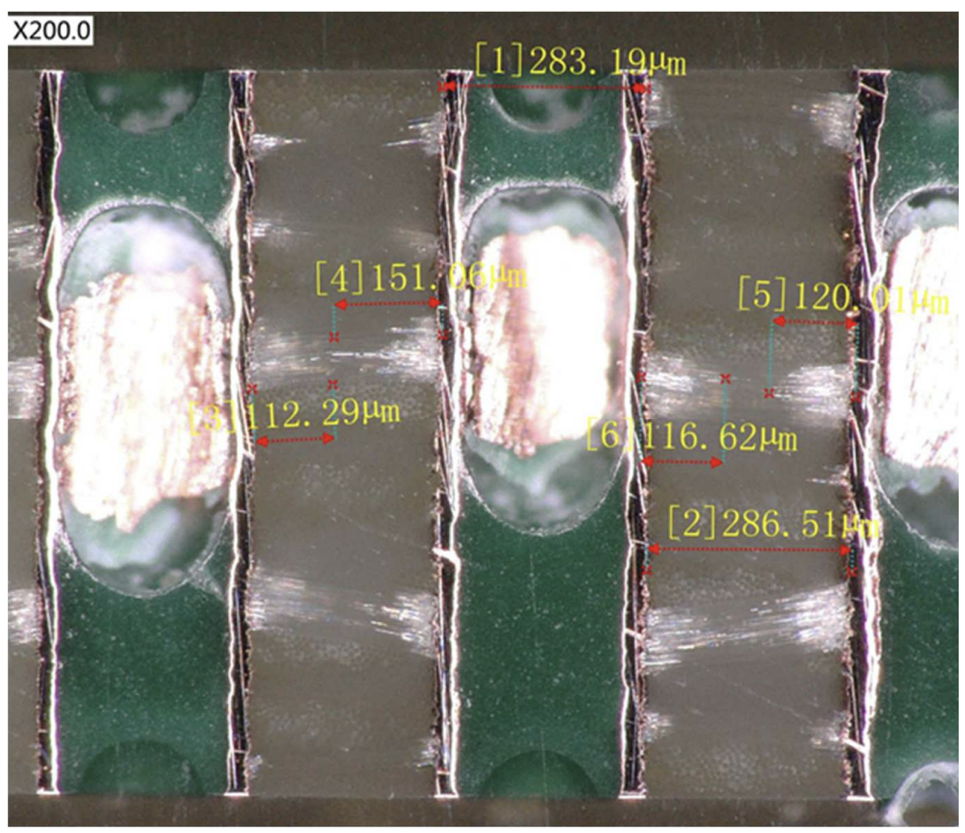
PCB ICD
What Is PCB ICD and How Does It Develop?
PCB ICD refers to an interconnect defect that compromises the electrical connection between conductive layers in a printed circuit board. In multilayer PCB manufacturing, inner-layer copper circuitry must connect reliably to plated through-holes or other interlayer structures. When the interface between the copper and the plated connection becomes damaged or separated, electrical continuity can become unstable or fail completely.
The term is commonly associated with inner-layer separation or a loss of reliable contact between inner-layer copper and the plated copper in a drilled hole. Such defects may develop when the copper-to-copper interface is weakened by inadequate surface preparation, contamination, excessive thermal stress, or unsuitable manufacturing conditions. The precise failure mechanism must be confirmed through inspection and analysis rather than assumed from electrical test results alone.
Unlike visible surface defects, these problems often occur inside the board, where they cannot be detected through a routine visual inspection. A PCB may pass initial electrical testing but develop an intermittent connection after repeated heating and cooling, soldering, or operation under load. This makes early process control and appropriate reliability testing particularly important.
Why PCB ICD Requires Attention in PCB Manufacturing
Interconnect defects deserve attention because they can remain hidden until a board experiences electrical or thermal stress. A weak copper interface may initially conduct electricity, yet its resistance can increase as the board expands and contracts during operation. In severe cases, the connection may become open-circuit, interrupting signals or power delivery.
The consequences depend on the application. In consumer electronics, an intermittent connection may cause unexpected resets or functional instability. In automotive electronics, industrial controls, telecommunications equipment, or other high-reliability systems, an internal connection failure can result in costly troubleshooting, field returns, and production interruptions.
Another challenge is that these defects may be difficult to identify by testing alone. A standard electrical continuity test can detect an open connection that already exists, but it may not reveal a latent defect that only appears after thermal cycling or other stress. Manufacturers therefore need a combination of process monitoring, appropriate inspection methods, and reliability testing based on the product’s risk level.
PCB ICD Causes: Common Problems During Production
Several manufacturing conditions can contribute to interconnect defects. One important factor is inadequate inner-layer copper preparation before lamination. If the copper surface is contaminated or the bonding interface is poorly prepared, the resulting structure may not withstand subsequent thermal stress. Inadequate cleaning, improper surface treatment, or inconsistent process control can increase the risk of weak interfaces.
Drilling and desmear processes are also important. Drilling generates heat and mechanical stress, while resin smear can cover copper at the hole wall and interfere with subsequent electrical connections if it is not properly removed. Poor drilling parameters, worn drill bits, unsuitable desmear conditions, or insufficient process control can compromise hole-wall quality and contribute to interconnect reliability problems.
Copper plating introduces another potential risk. If the hole wall is inadequately prepared or the plating process produces insufficient copper thickness, poor adhesion, or localized discontinuities, the finished interconnect may be vulnerable to failure. Excessive thermal exposure during multilayer lamination, soldering, or assembly can further stress an already weak interface.
These causes should not be treated as interchangeable. Inner-layer separation, resin smear, plating defects, and thermal cracking are different failure mechanisms that may produce similar electrical symptoms. Accurate diagnosis is therefore necessary before corrective action is selected.
PCB ICD Cost Factors: What Drives Manufacturing and Quality Costs?
The cost of preventing and managing interconnect defects extends beyond the price of the PCB itself. The main cost factors include material selection, process capability, inspection requirements, reliability testing, and the potential expense of scrapped boards or customer returns.
Material and design costs can increase when a product requires specialized laminate systems, more demanding thermal performance, or tighter manufacturing tolerances. These choices may be justified for high-layer-count boards, fine-pitch designs, and applications exposed to repeated thermal cycling. However, the material alone cannot guarantee reliability if the manufacturing process is poorly controlled.
Manufacturing and inspection costs depend on the number of layers, via structures, copper requirements, drilling complexity, and process-control standards. More demanding designs may require closer monitoring of drilling, desmear, plating, lamination, and thermal processing. Additional microsection analysis or other targeted inspections can increase upfront costs, but they may help identify defects before boards reach assembly.
Failure-related costs can be considerably higher than preventive measures. A defective board may require rework where feasible, replacement, additional testing, or complete scrapping. If the issue reaches the customer, the resulting costs can include returned products, production downtime, warranty claims, and damage to supplier relationships.
The most effective cost strategy is to balance prevention with risk-based verification. Cutting essential process controls to reduce the unit price can create larger expenses later, especially when defects are difficult to detect after assembly.
PCB ICD Impact on Electrical Performance and Product Reliability
The most direct impact is a loss of reliable electrical continuity between conductive layers. When an interconnect becomes unstable, current may be interrupted or resistance may increase. In power circuits, this can cause voltage drops, localized heating, or intermittent operation. In signal circuits, an unstable connection may produce signal interruptions, timing errors, or unexpected system behavior.
High-speed and high-frequency designs require particular attention because interconnect structures are part of the overall signal path. Although signal integrity also depends on impedance, dielectric properties, routing geometry, and other factors, a defective interlayer connection can introduce discontinuities that undermine predictable electrical performance.
Thermal and mechanical reliability are equally important. Copper and laminate materials expand at different rates as temperature changes. Repeated thermal cycles can place stress on plated holes and copper interfaces, potentially extending an existing defect or causing a marginal connection to fail. Boards used in power electronics, automotive systems, and industrial environments may face especially demanding conditions.
The reliability impact is not limited to the first failed board. If a defect results from a systematic process issue, multiple boards from the same production lot may be affected. Identifying the root cause early helps manufacturers contain the risk, avoid repeated failures, and protect the consistency of subsequent production batches.
PCB ICD Prevention: Practical Solutions for Manufacturers
Preventing interconnect defects begins with controlling the manufacturing process at every critical stage. Before lamination, inner-layer copper surfaces must be clean and properly prepared. Manufacturers should monitor cleaning effectiveness, surface treatment consistency, material handling, and lamination conditions to support a stable copper-to-resin and copper-to-copper structure.
During drilling, appropriate tool selection, drill-life management, and parameter control help reduce mechanical damage and excessive heat. Desmear must remove resin residue from hole walls without damaging the surrounding material or compromising the copper interface. The correct process window depends on the laminate system, hole geometry, and board construction, so settings should be validated rather than copied blindly between designs.
For plating, effective hole-wall preparation and consistent copper deposition are essential. Manufacturers should monitor plating chemistry, process uniformity, copper thickness, and relevant production records. Where the design or reliability requirements justify it, cross-sectional microsection analysis can help evaluate hole-wall condition, copper coverage, and potential separation at interconnect interfaces.
When a defect is detected, the response should include containment, failure analysis, corrective action, and verification. Electrical retesting alone may not establish the root cause. Depending on the suspected mechanism, manufacturers may need microsectioning, metallographic examination, thermal stress testing, or other appropriate analyses. Corrective actions should then be confirmed through documented process results and follow-up inspections.
Finally, engineers and PCB manufacturers should review stack-up design, via structures, copper requirements, and expected operating temperatures before production begins. Clear design rules and communication between the customer and manufacturer can reduce avoidable risks and prevent late-stage changes that increase cost and delay delivery.
Conclusion
Interconnect defects are a significant reliability concern because they can remain hidden inside a multilayer PCB while weakening the electrical connection between conductive layers. Their effects range from intermittent operation and signal disruption to complete circuit failure. Since several different manufacturing problems can produce similar symptoms, effective prevention requires accurate diagnosis, disciplined process control, and verification appropriate to the product’s intended use.
For PCB designers and purchasing teams, reliability should be evaluated alongside price, lead time, and manufacturing capability. A qualified supplier should be able to explain its controls for lamination, drilling, desmear, plating, inspection, and failure analysis rather than relying solely on a final electrical test.
SQ PCB emphasizes the importance of manufacturing consistency, process monitoring, and quality verification in custom PCB production. By working closely with customers to review design requirements and manufacturing risks, PCB suppliers can help reduce avoidable defects and improve production consistency. Ultimately, preventing interconnect failures is not just a matter of passing inspection; it is about ensuring that the finished board performs reliably throughout its intended service life.
FAQs
1. What does PCB ICD mean?
PCB ICD stands for Interconnect Defect. It generally refers to a defect that compromises the electrical connection between conductive layers or interconnect structures within a printed circuit board. The exact failure mechanism should be confirmed through appropriate inspection and analysis.
2. What causes interconnect defects in multilayer PCBs?
Common contributing factors include inadequate copper surface preparation, contamination, poor drilling conditions, incomplete desmear, plating defects, and excessive thermal stress. The actual cause depends on the board construction and the location and characteristics of the defect.
3. Can PCB ICD pass electrical testing?
Yes. A latent defect may initially maintain electrical continuity and only become apparent after thermal cycling, soldering, or operation under stress. Appropriate process controls and risk-based reliability testing can help detect weaknesses that a basic continuity test may miss.
4. How can manufacturers prevent interconnect defects?
Manufacturers can reduce risk through proper copper surface preparation, controlled lamination, optimized drilling and desmear, consistent copper plating, and appropriate inspection. Root-cause analysis and verification of corrective actions are essential when a defect is identified.
5. Does PCB ICD increase the total cost of PCB manufacturing?
It can. Prevention may require additional process controls, inspection, or reliability testing, but these measures can reduce scrap, rework, production delays, warranty claims, and field failures. The most economical approach is to match preventive controls to the board’s design complexity and reliability requirements.

- Special PCB
- long board pcb
- Flexible PCBs
- Special PCB
- Express Printed Circuit Board
- Pcb Prototype
- LED PCB
- PCB
- Pcb Meaning
- Printed Circuit Board
- Pcb manufacturer
- Rigid pcb board
 Quote
 E-mail